Process for Producing Group 13 Metal Nitride, and Seed Crystal Substrate for Use in Same
- Summary
- Abstract
- Description
- Claims
- Application Information
AI Technical Summary
Benefits of technology
Problems solved by technology
Method used
Image
Examples
example 1
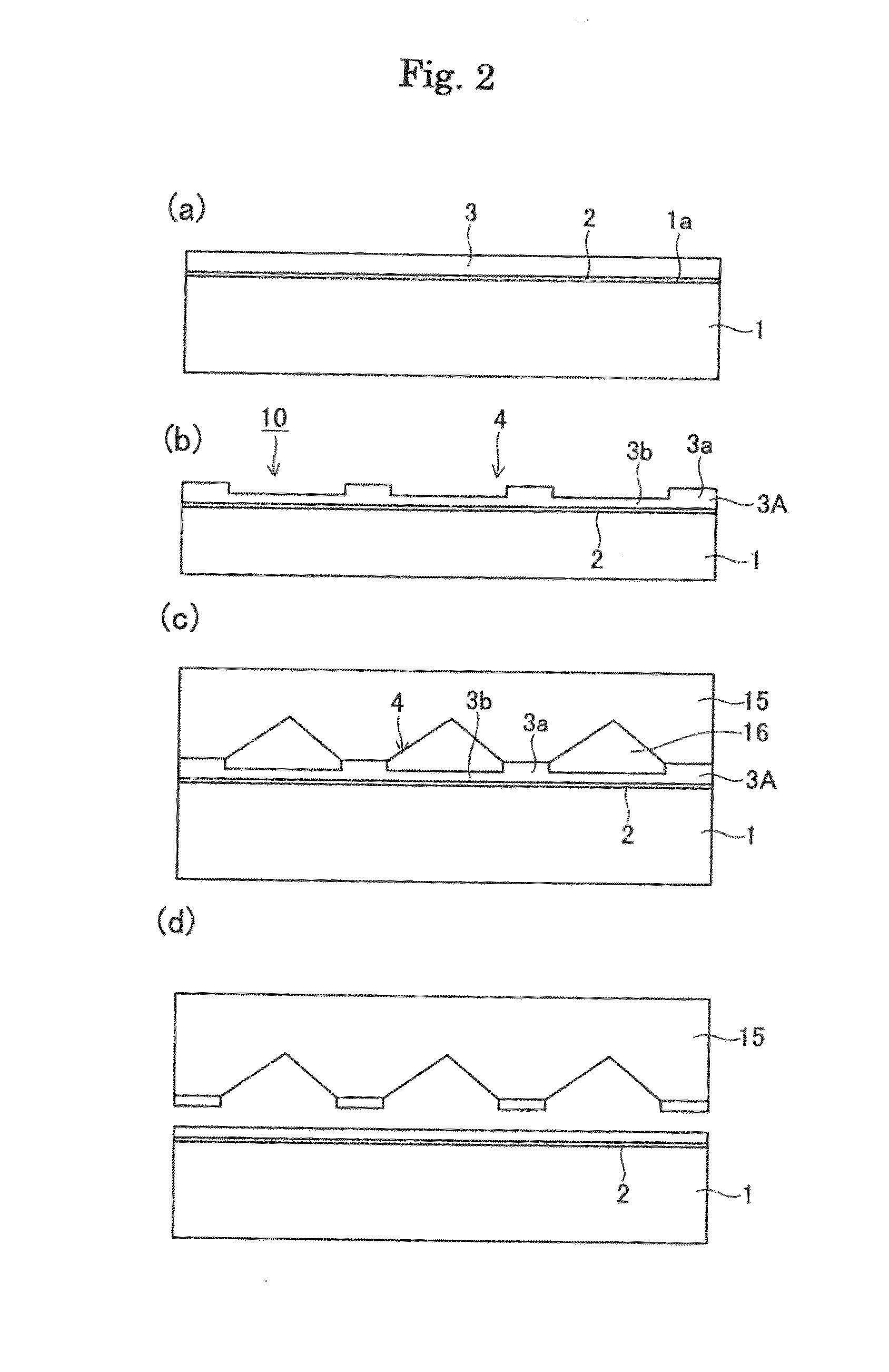
[0068]Gallium nitride single crystal was grown according to the method described referring to FIGS. 2 and 3.
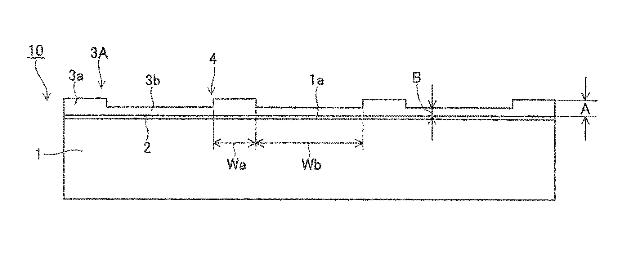
[0069]Specifically, it was prepared a so-called GaN template in which a seed crystal layer 3 with a thickness of 5 μm and composed of gallium nitride single crystal was epitaxially grown by MOCVD method on a surface of a c-face sapphire body 1 having a diameter of 3 inches. In a central region of φ54 mm of the surface of the template, stripe-shaped Ni thin films (resists) each having a width of 0.05 mm were formed by electron beam deposition at a period of 0.55 mm. The thickness of the Ni thin film was made 4000 angstroms. At this time, the direction of each stripe was made parallel with the direction of a-axis (11-20) of sapphire forming the supporting body 1. The seed crystal film 3 was dry-etched by using ICP-RIE system and chlorine gas to a depth of 4 μm. Thereafter, the Ni thin films were removed using commercial etchant. The substrate was then washed using buffered fluor...
example 2
[0074]The experiment of growing gallium nitride single crystal was performed according to the same procedure as the Example 1.
[0075]According to the present example, however, the thickness “A” of the main body parts, the thickness “B” of the thin parts, and dimension of the step (A-B) were changed. The results were shown in table 2.
TABLE 2Presence orabsence ofThickness ofpeeling overPresence orABA − Bgrown crystalwhole surfaceAbsence of(μm)(μm)(μm)(μm)of sapphireCracks50.54.51.2~1.5PresentThree lines8171.3~1.9PresentTwo lines80.57.51.6~2.3PresentFive lines51.53.51.0~1.5PresentNone3121.1~1.9PresentTwo lines
[0076]In all the cases, GaN crystal was grown in a thickness of about 1.5 μm. Cracks were not present in one example, and several lines of small cracks were generated in the remaining ones, and the underlying sapphire body was peeled off over the whole surface in each. FIG. 7 schematically shows the state of generation of cracks “C”. Cracks of about 1 cm were generated in the outer...
PUM
 Abstract
Description
Claims
Application Information
 - R&D Engineer
- R&D Manager
- IP Professional
- Industry Leading Data Capabilities
- Powerful AI technology
- Patent DNA Extraction
Browse by: Latest US Patents, China's latest patents, Technical Efficacy Thesaurus, Application Domain, Technology Topic, Popular Technical Reports.
© 2024 PatSnap. All rights reserved.Legal|Privacy policy|Modern Slavery Act Transparency Statement|Sitemap|About US| Contact US: help@patsnap.com


