Organic electroluminescent element

a technology of electroluminescent elements and organic materials, applied in the direction of solid-state devices, semiconductor devices, thermoelectric devices, etc., can solve the problems of increased operation voltage, undesired increase in voltage, short circuits, etc., to achieve superior long-term durability and lifetime characteristics, and suppress the direct reaction of mixed layers

Active Publication Date: 2014-01-16
SAMSUNG DISPLAY CO LTD
View PDF3 Cites 10 Cited by
  • Summary
  • Abstract
  • Description
  • Claims
  • Application Information

AI Technical Summary

Benefits of technology

[0029]It is possible according to the present invention to suppress direct reaction of the mixed layer containing an electron-donating substance and an electron-transporting organic material with the hole-injection layer and to inhibit mixing of the interface between the mixed layer and the hole-injection layer and diffusion of materials between the layers during operation. It is thus possible to obtain an organic electroluminescent element superior in long-term durability and lifetime characteristics.

Problems solved by technology

However, as described above, installation of an intermediate layer separating multiple light-emitting layers may lead to an increase in operation voltage and an undesired increase in voltage, and also may cause defects such as short circuits due to deterioration in film quality.
Specifically in the case of the intermediate layer of the type (1), there is a concern about the defects caused by short circuits due to the poor quality of the V2O5 layer.
Further in the case of the type (2), there may be a problem of increase in voltage caused by the side reactions between the two layers.

Method used


Image

  • Organic electroluminescent element
  • Organic electroluminescent element
  • Organic electroluminescent element

Examples


example 1

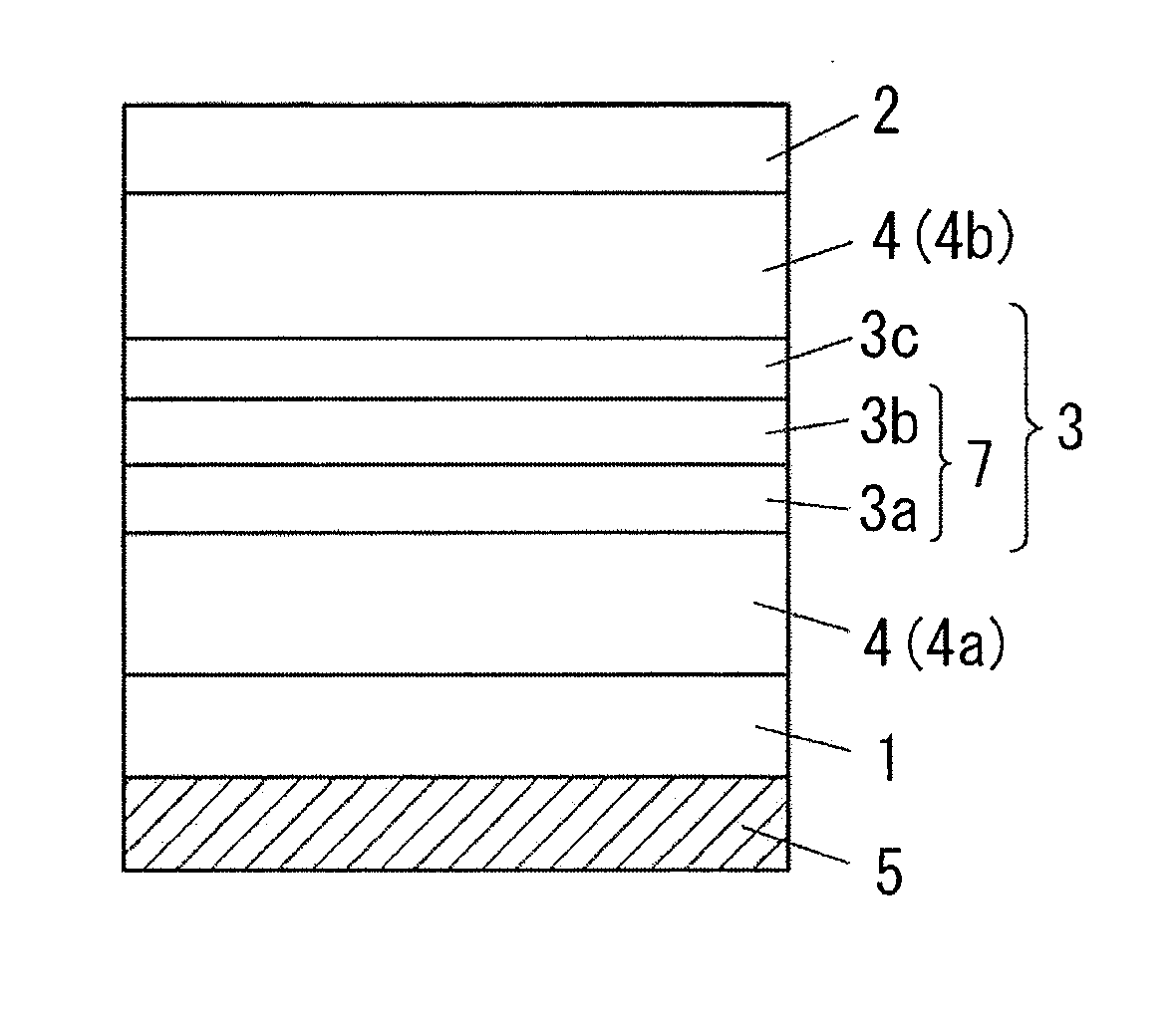
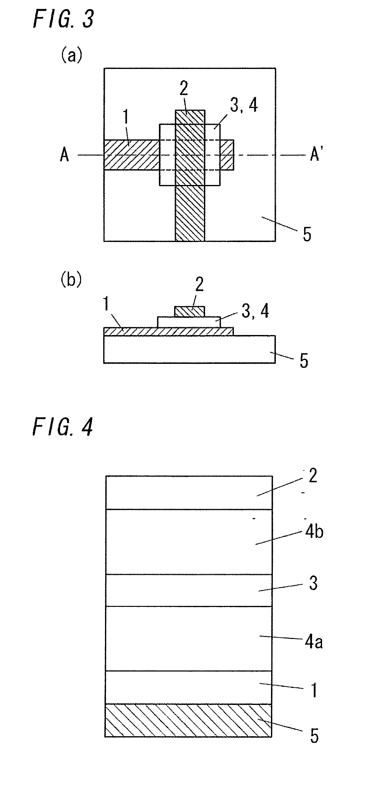
[0075]First, as shown by the pattern of FIG. 3, a glass substrate 5 having a thickness of 0.7 mm carrying an ITO film, which has a thickness of 150 nm, a width of 5 mm, and a sheet resistance of about 10 Ω / □, formed as a positive electrode 1 thereon was prepared. The substrate 5 was previously washed with detergent, ion-exchange water, and acetone respectively for 10 minutes under ultrasonication, vapor-washed with IPA (isopropyl alcohol), dried and additionally subjected to UV / O3 treatment.

[0076]The substrate 5 was then fixed in a vacuum evaporator and a film of 4,4′-bis[N-(naphthyl-N-phenyl-amino]biphenyl (α-NPD) and tetrafluoro-tetracyano-quinodimethane (F4-TCNQ) (molar ratio 1:1) having a thickness of 30 nm was formed as a hole-injection layer, on the surface of the positive electrode 1 formed on the substrate 5, by co-vapor deposition in a reduced-pressure atmosphere at 1×10⁻⁴ Pa or less. Next, a film of α-NPD having a thickness of 30 nm was formed as hole-transporting layer on...

example 2

[0086]An organic electroluminescent element was prepared in a manner similar to Example 1, except that, in preparation of the mixed layer 3a of intermediate layer 3, a film of BCP having a thickness of 9 nm was first formed on the electron-transporting layer and a film of Li having a thickness of 1 nm was formed thereon, to give a mixed layer 3a containing an electron-donating substance (Li) and an electron-transporting organic material (BCP).


PUM


Abstract

Provided is an organic electroluminescent element superior in long-term durability and lifetime characteristics. The organic electroluminescent element has a structure where plurality of light-emitting layers formed via an intermediate layer are interposed between a positive electrode and a negative electrode. The intermediate layer has a mixed layer, a first layer, and a hole-injection layer which are formed in this order from the positive electrode to the negative electrode, the mixed layer containing an electron-donating substance and an electron-transporting organic material, and the first layer being made of an electron-transporting material. The first layer has a thickness in a range of 0.2 to 2.0 nm. The hole-injection layer consists of an electro-accepting organic material.

Description

TECHNICAL FIELD[0001]The present invention relates to an organic electroluminescent element available for light sources for lighting use, backlights for liquid crystal displays, flat panel displays and others.BACKGROUND ART[0002]A known example of organic light-emitting elements, so-called organic electroluminescent elements, is an element that has a transparent electrode serving as a positive electrode, a hole-transporting layer, a light-emitting layer (organic light-emitting layer), an electron-injection layer, and an electrode serving as a negative electrode stacked in this order on a surface of a transparent substrate. When voltage is applied between the positive and negative electrodes, the electrons injected into the light-emitting layer via the electron-injection layer and the holes injected into the light-emitting layer via the hole-transporting layer recombines with each other, and this recombination causes light in the light-emitting layer, and the light generated in the l...

Claims


Application Information

Patent Timeline
Patent Type & Authority Applications(United States)
IPC IPC(8): H01L51/50
CPCH01L51/5008H10K50/131H10K50/19H10K30/865
Inventor IDE, NOBUHIROITO, NORIHIROTSUJI, HIROYASUZUKA, YUKO
Owner SAMSUNG DISPLAY CO LTD
Why Eureka
Try Eureka