Eureka AIR delivers breakthrough ideas for toughest innovation challenges, trusted by R&D personnel around the world.

Method for Manufacturing Liquid Crystal Display Device and Liquid Crystal Display Device

a liquid crystal display and liquid crystal technology, applied in semiconductor devices, instruments, optics, etc., can solve the problems of difficult control of the amount of liquid crystal filled, affecting the manufacturing performance, and the vacuum filling process takes more and more time to compl

Active Publication Date: 2013-11-14
SHENZHEN CHINA STAR OPTOELECTRONICS TECH CO LTD
View PDF2 Cites 1 Cited by
  • Summary
  • Abstract
  • Description
  • Claims
  • Application Information

AI Technical Summary

Benefits of technology

The present invention describes a method for manufacturing a liquid crystal display device with an enclosing resin that can adjust the amount of liquid crystal between TFT and CF substrates to prevent thermal deformation. This method involves directly forming an enclosing resin frame body with an entry opening and a recoverable closing section. The closing section can be removed to expel excessive liquid crystal and then repaired, simplifying the operation and reducing the cost of re-working. The technical effect of this invention is to provide a simple and effective solution to prevent thermal deformation of the substrates and reduce the cost for re-working.

Problems solved by technology

However, with the increase of the size of the liquid crystal display device, the vacuum filling process takes more and more time to complete.
The severely affects the manufacture performance.
It is, however, generally difficult to control the amount of liquid crystal filled in the process of filling liquid crystal with the distribution method.
This will cause abnormal conditions of for example inhomogeneous displaying color.

Method used


Image

  • Method for Manufacturing Liquid Crystal Display Device and Liquid Crystal Display Device
  • Method for Manufacturing Liquid Crystal Display Device and Liquid Crystal Display Device
  • Method for Manufacturing Liquid Crystal Display Device and Liquid Crystal Display Device

Examples


Embodiment Construction

[0040]To further expound the technical solution adopted in the present invention and the advantages thereof, a detailed description is given to a preferred embodiment of the present invention and the attached drawings.

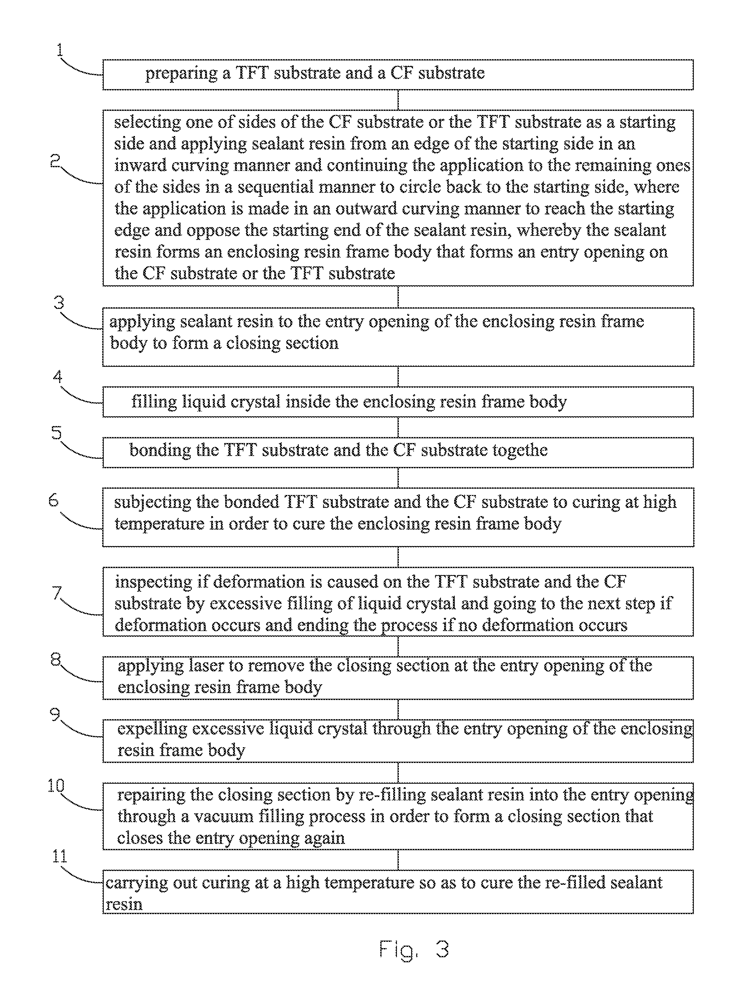
[0041]Referring to FIG. 3, as well as FIGS. 4 and 5, the present invention provides a method for manufacturing a liquid crystal display device, which comprises the following steps:

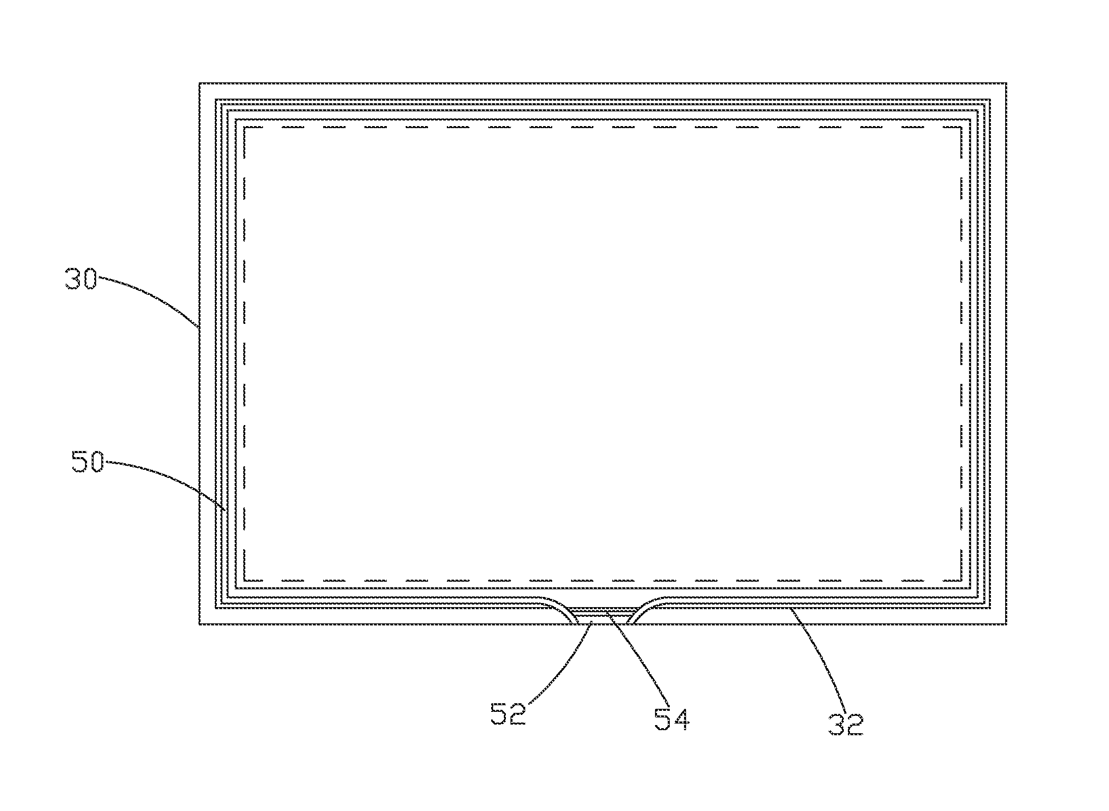
[0042]Step 1: preparing a TFT substrate 20 and a CF substrate 30. The CF substrate 30 comprises a black matrix 32 formed thereon.

[0043]The TFT substrate 20 and the CF substrate 30 are manufactured through the operations of thin film, yellow light, etching, and film stripping and the specific operations used can be any of the known operations.

[0044]Step 2: selecting one of sides of the CF substrate 30 or the TFT substrate 20 as a starting side and applying sealant resin from an edge of the starting side in an inward curving manner and continuing the application to the remaining ones of the sid...


PUM


Abstract

The present invention provides a method for manufacturing a liquid crystal display device and a liquid crystal display device. The method includes (1) preparing a TFT substrate and a CF substrate; (2) applying sealant resin to the TFT substrate or CF substrate to form an enclosing resin frame body that forms an entry opening on the CF substrate or the TFT substrate; (3) applying sealant resin to the entry opening of the enclosing resin frame body to form a closing section; (4) filling liquid crystal inside the enclosing resin frame body; (5) bonding the TFT substrate and the CF substrate together; and (6) subjecting the bonded TFT substrate and the CF substrate to curing at high temperature in order to cure the enclosing resin frame body.

Description

BACKGROUND OF THE INVENTION[0001]1. Field of the Invention[0002]The present invention relates to the field of manufacture of liquid crystal display device, and in particular to a method for manufacturing a liquid crystal display device and a liquid crystal display device.[0003]2. The Related Arts[0004]Liquid crystal display (LCD) has a variety of advantages, such as thin device body, low power consumption, and being free of radiation, and is thus widely used. Most of the LCDs that are currently available in the market are backlighting LCDs, which comprise a liquid crystal display panel and a backlight module. The working principle of the liquid crystal display panel is that liquid crystal polymer molecules interposed between two parallel glass substrates and a plurality of vertical and horizontal fine electrical wires is arranged between the two glass substrates, whereby the liquid crystal molecules are controlled to change direction by application of electricity in order to refract...

Claims


Application Information

Patent Timeline
IPC IPC(8): G02F1/1339H01L33/52H01L33/50
CPCG02F1/1339G02F1/1341G02F1/13415
Inventor LEE, KUANCHENGLI, CHIHHSIEN
Owner SHENZHEN CHINA STAR OPTOELECTRONICS TECH CO LTD
Why Eureka
Eureka Blog
Learn More