
Organic Light Emitting Diode Display

a light-emitting diode and organic technology, applied in the direction of transistors, solid-state devices, thermoelectric devices, etc., can solve the problems of voltage drop generation in the wires, quality deterioration such as stains, and achieve the effect of improving display quality

Active Publication Date: 2013-08-15
SAMSUNG DISPLAY CO LTD
View PDF5 Cites 35 Cited by
  • Summary
  • Abstract
  • Description
  • Claims
  • Application Information

AI Technical Summary

Benefits of technology

This patent describes a way to make a high-quality organic light emitting diode (OLED) display. The technology improves the display by using a special process. The result is a display that is more clear and accurate, which makes it easier to see information.

Problems solved by technology

However, as demands for high-resolution displays have increased, the numbers of gate wires, data wires, pixel circuits, and organic light emitting diodes included in the organic light emitting diode (OLED) display have also increased, so various problems such as distribution of the wires (particularly the gate wires outnumbering the data wires), generation of voltage drop in the wires, and quality deterioration such as stains.

Method used


Image

  • Organic Light Emitting Diode Display
  • Organic Light Emitting Diode Display
  • Organic Light Emitting Diode Display

Examples


Embodiment Construction

[0041]The present invention will be described more fully hereinafter with reference to the accompanying drawings, in which exemplary embodiments of the invention are shown. As those skilled in the art would realize, the described embodiments maybe modified in various different ways, all without departing from the spirit or scope of the present invention.

[0042]Parts that are irrelevant to the description are omitted in order to clearly describe the present invention, and like reference numerals designate like elements throughout the specification.

[0043]In various exemplary embodiments, the same reference numerals are used for elements having the same configurations and will be representatively described in a first exemplary embodiment, and in other exemplary embodiments, only elements different from those of the first exemplary embodiment will be described.

[0044]The size and thickness of the components shown the drawings are optionally determined for better understanding and ease of ...


PUM


Abstract

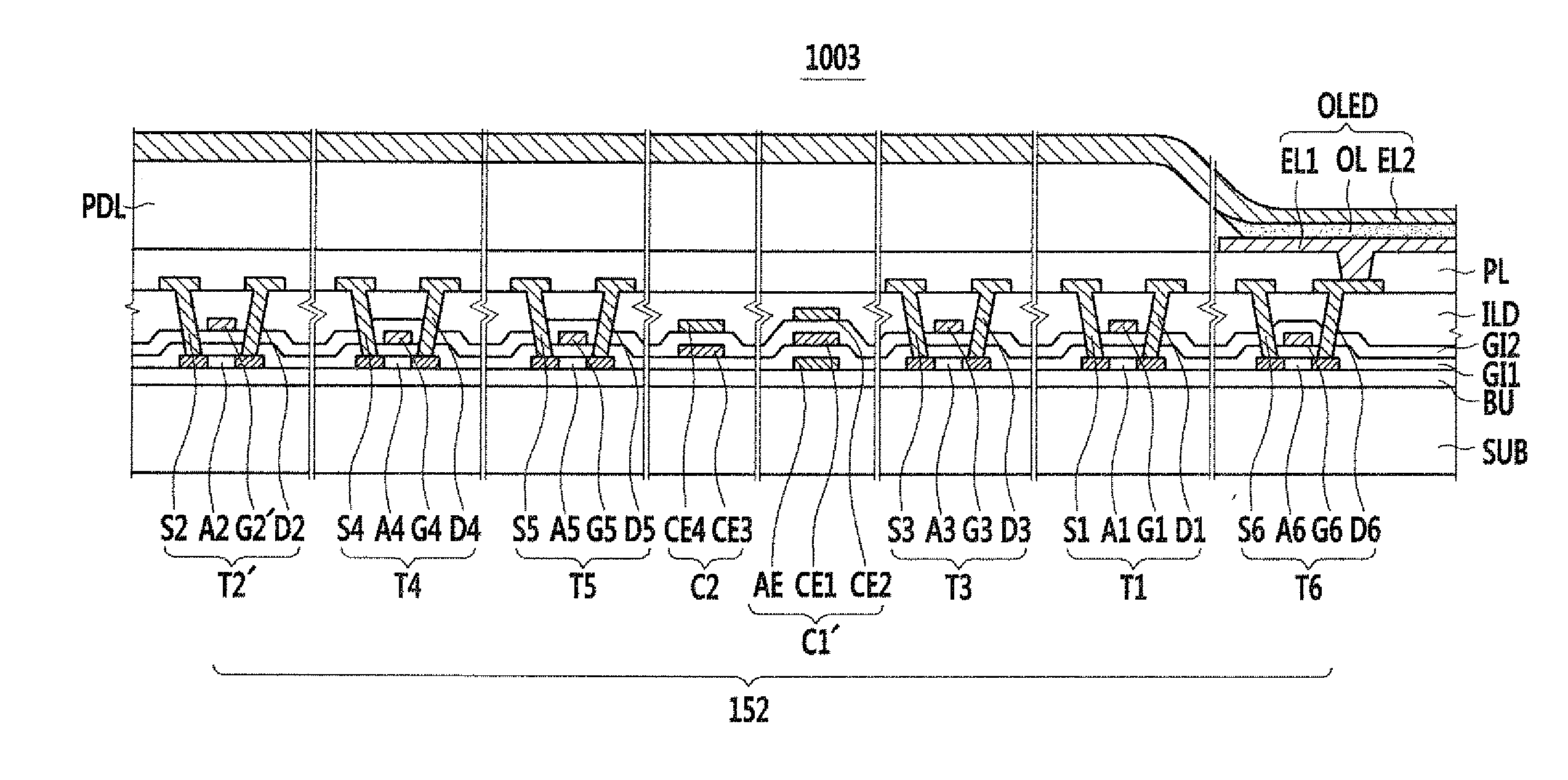
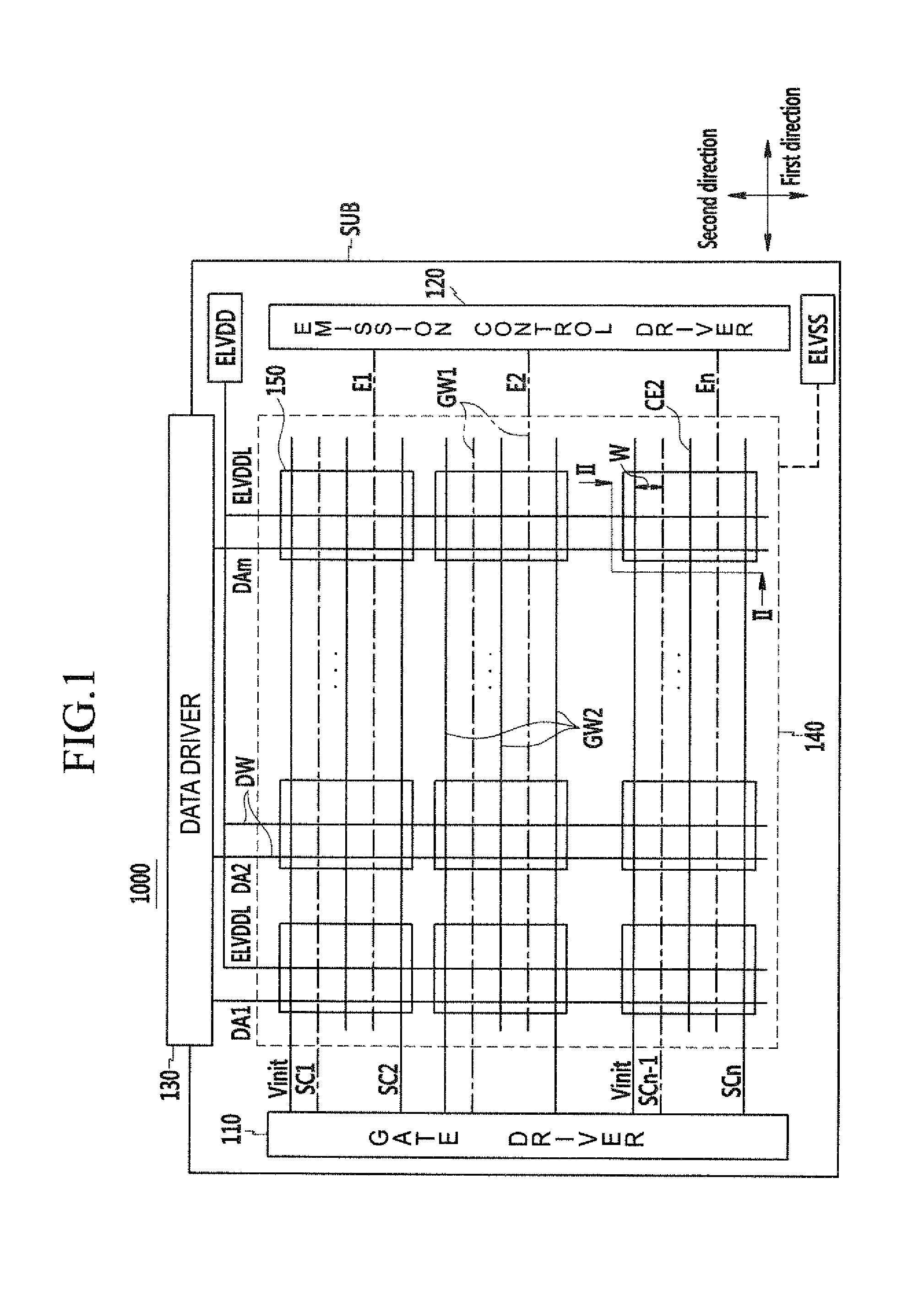
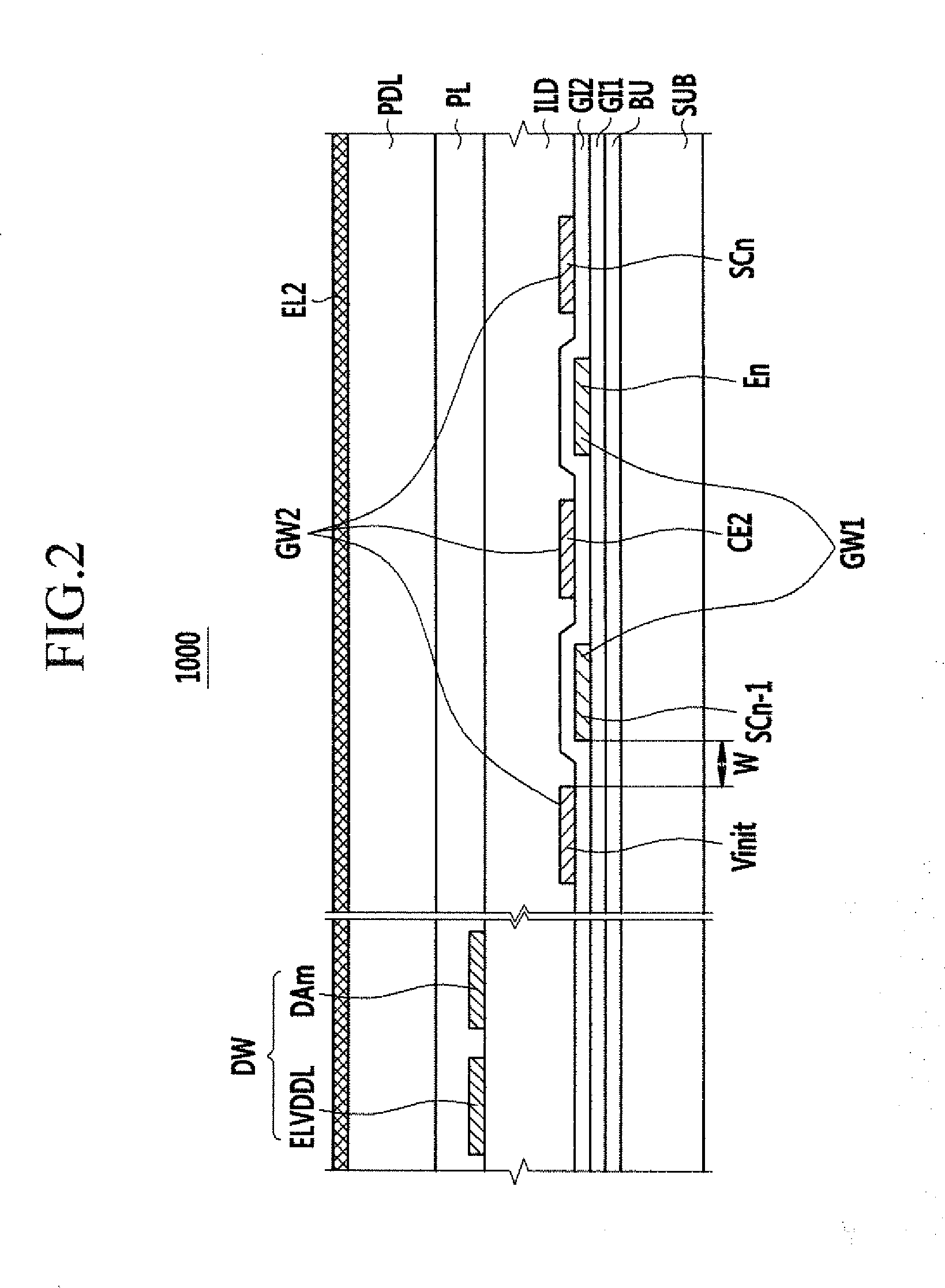
An organic light emitting diode display includes: first gate wires provided on a substrate with a first insulation layer therebetween and extended in a first direction; second gate wires provided on a second insulation layer above the first insulation layer and extended in the first direction; data wires provided on a third insulation layer above the second insulation layer and extended in a second direction crossing the first direction; a pixel circuit connected to the first gate wires, the second gate wires, and the data wires; and an organic light emitting diode connected to the pixel circuit.

Description

CLAIM OF PRIORITY[0001]This application makes reference to, incorporates the same herein, and claims all benefits accruing under 35 U.S.C. §119 from an application earlier filed in the Korean Intellectual Property Office on the 10 Feb. 2012 and there duly assigned Serial No. 10-2012-0013837.BACKGROUND OF THE INVENTION[0002]1. Field of the Invention[0003]The described technology relates generally to an organic light emitting diode (OLED) display. More particularly, the described technology relates generally to an organic light emitting diode (OLED) display including a pixel circuit having a plurality of thin film transistors and at least one capacitor.[0004]2. Description of the Related Art[0005]A display device is a device for displaying images, and recently, a display device including an organic light emitting diode (OLED) has come to prominence.[0006]Unlike a liquid crystal display (LCD), the OLED has the characteristic of self-emission and does not require a light source, so the ...

Claims


Application Information

Patent Timeline
IPC IPC(8): H01L27/32
CPCH01L27/3276H10K59/131H01L2027/11879H10K30/865
Inventor AN, CHI-WOOKTAE, SEUNG-GYULEE
Owner SAMSUNG DISPLAY CO LTD
Learn More