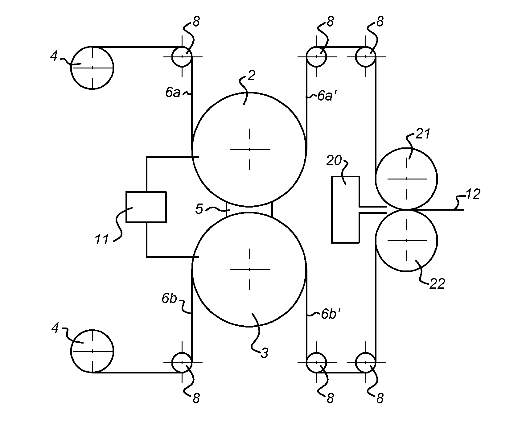
Method for Manufacturing a Barrier Layer on a Substrate and a Multi-Layer Stack
a technology of barrier layer and multi-layer stack, which is applied in the direction of coatings, chemical vapor deposition coatings, semiconductor devices, etc., can solve the problem of not revealing the conditions for creating an improved barrier layer, and achieve good handling properties, good barrier properties, and cost-effective
- Summary
- Abstract
- Description
- Claims
- Application Information
AI Technical Summary
Benefits of technology
Problems solved by technology
Method used
Image

Examples
example 1-11
[0060]All electrode couples 2, 3 have been independently dynamically matched to an own power-supply. The power was continuously supplied to each unit (AC / 800 W / 200 kHz). As precursor in each treatment space 5, 2 ppm TEOS was used.
[0061]The gas mixture in each treatment space contained a O2 / N2-mixture and is respectively controlled on 10% / 90% except for examples 8, 9, 10 and 11.
[0062]Example 8 used in each treatment space a O2 / N2-mixture and is respectively controlled on 6% / 94%.
[0063]Example 9 used in each treatment space a O2 / N2-mixture and is respectively controlled on 1% / 99%.
[0064]Example 10 and 11 used in each treatment space common air as gas-mixture. Further in each example conditions in the treatment spaces 5 were kept the same. As substrate 6a,6b PET ST505 (Melinex) from DuPont Tejin Films (width 20 cm / thickness 100 μm) was used.
example 3
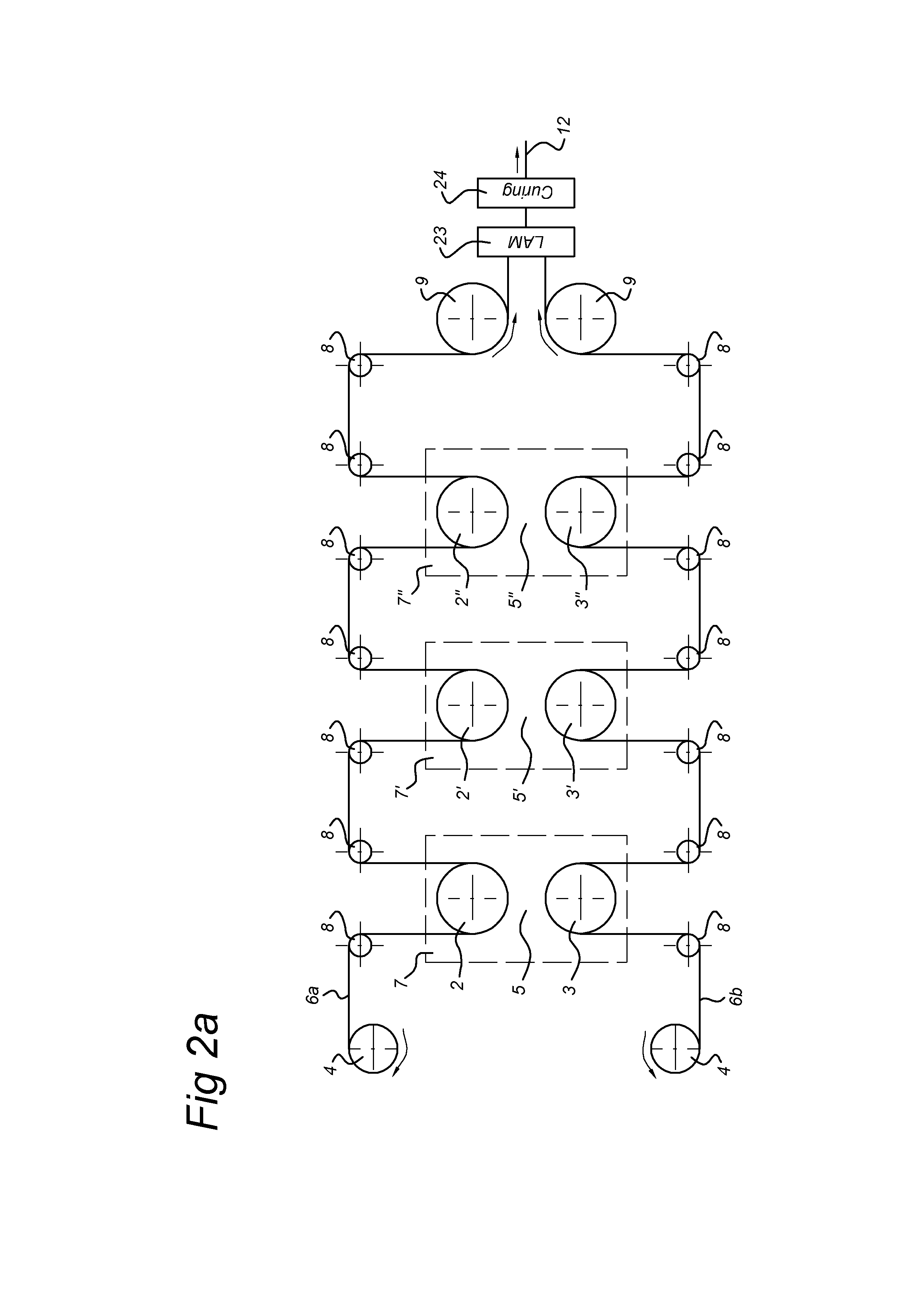
[0069]Two barrier films 14 are deposited simultaneously using the set-up as shown in FIG. 2a using an atmospheric pressure plasma device 10 and three subsequent treatment spaces resulting in two substrates having both a SiOx-barrier layer of 450 nm.
[0070]Treatment space conditions were same as in example 1 conditions however the line speed of the substrates was 200% higher as in example 1.
[0071]The substrates are brought together with the facing side to each other and laminated with a hydrophobic acrylate of 10 micron which was followed by UV-curing.
[0072]The resulted multi-layer stack shows no crack-defects and has a WVTR of 1.3*10−3 g / m2.day.
example 4
[0073]Two barrier films 14 are deposited simultaneously using the set-up as shown in FIG. 2a except the substrates were fed using four subsequent treatment spaces using an atmospheric pressure plasma device 10 resulting in two substrates having both a SiOx-barrier layer of 450 nm.
[0074]Treatment space conditions were same as in example 1 conditions however the line speed of the substrates was 300% higher as in example 1.
[0075]The substrates are brought together with the facing side to each other and laminated with a hydrophobic acrylate of 10 micron which was followed by UV-curing.
[0076]The resulted multi-layer stack shows no crack-defects and has a WVTR of about 9.6*10−4 g / m2.day.
PUM
| Property | Measurement | Unit |
|---|---|---|
| Fraction | aaaaa | aaaaa |
| Fraction | aaaaa | aaaaa |
| Thickness | aaaaa | aaaaa |
Abstract
Description
Claims
Application Information
 - R&D
- Intellectual Property
- Life Sciences
- Materials
- Tech Scout
- Unparalleled Data Quality
- Higher Quality Content
- 60% Fewer Hallucinations
Browse by: Latest US Patents, China's latest patents, Technical Efficacy Thesaurus, Application Domain, Technology Topic, Popular Technical Reports.
© 2025 PatSnap. All rights reserved.Legal|Privacy policy|Modern Slavery Act Transparency Statement|Sitemap|About US| Contact US: help@patsnap.com