Backlight module for providing light to a display panel and display device therewith

a backlight module and display panel technology, applied in the field of backlight modules, can solve the problems of poor image quality, distance a, area aa, and distance a, and achieve the effects of reducing labor hours, preventing hot spots, and reducing manufacturing costs

Active Publication Date: 2013-06-06
WISTRON CORP
View PDF1 Cites 2 Cited by
  • Summary
  • Abstract
  • Description
  • Claims
  • Application Information

AI Technical Summary

Benefits of technology

[0016]Since the optical material layer of the present invention is disposed between the frame and the display panel, the optical material layer of the present invention does not contact the light guide plate directly. Accordingly, it can prevent the optical material layer from scratching the light guide plate. Furthermore, since the optical material layer is disposed above the frame instead of being covered on the light guide plate, part of the light emitted from the light emitting unit will be absorbed by the frame. Further, since there is air between the optical material layer and the light guide plate, it can prevent hot spots resulting from prism effect of the light emitted from the light emitting unit in the prior art. In such a manner, there is no need to dispose additional micro-structures on the light guide plate for making the light guide plate illuminate uniformly. Accordingly, it can reduce manufacture cost. Since the hot spot issue can be solved, the end of the frame can be designed to be aligned with a boundary of the active area of the display panel without overlapping. As a result, it can be implemented in the thin rim design. Since the stacking structure of the optical material layer of the present invention solves the hot spot issue, the present invention does not need to be constrained by the conventional A / P ratio. In other words, if the amount of the light emitting diodes of the light emitting unit is curtailed in consideration of cost, power consumption, heat dissipation and environment protection, the gap between the two adjacent light emitting diodes of the light emitting unit increases. Since the present invention is not constrained by the conventional A / P ratio, there is no need to increase the distance between the illuminating surface of the light emitting diode and the boundary of the active area. In such a manner, it can be implemented in the thin rim design. Furthermore, the optical material layer is disposed above the frame instead of utilizing the plastic frame to press and fix the optical material layer and the light guide plate. Accordingly, it is not required to detach the frame as the optical material layer needs to be reworked for replacement, so as to reduce labor hours and increase convenience of assembly. In summary, the present invention is capable of providing a liquid crystal display device with high assembly yield and convenience of assembly to meet the requirements of a thin size, such as the thin rim design, as well as good image quality for the consumer products in the market.

Problems solved by technology

Conversely, the smaller the ratio of A / P is, the worse the image quality will be.
In other words, in the situation of the high ratio of A / P, the light guide plate can provide more uniform light to the active area AA, while in the situation of the low ratio of A / P, non-uniform light on the active area AA provided by the light guide plate may occur, so as to result in hot spots.
However, the distance A, which is between the illuminating surface of the light emitting diode and the active area AA of the display panel projecting to the light guide plate, can not increase due to structural limitation.
As a result, the ratio of A / P can not be enhanced resulting in decrease of the image quality.
On the other hand, the increased distance A can not meet requirement of thin rim design.
Since the optical material layer contacts the light guide plate directly, scratches often occur on the optical material layer and / or the light guide plate.
As a result, it can not meet the requirement of thin rim design.
Accordingly, it is necessary to detach the plastic frame as replacing the optical material layer, so as to increase labor hours and result in inconvenience of assembly.
Therefore, how to provide a liquid crystal display device with a high assembly yield and convenience of assembly to meet the requirement of a thin size, such as the thin rim design, has become an issue of mechanical design for the consumer products in the market.

Method used


Image

  • Backlight module for providing light to a display panel and display device therewith
  • Backlight module for providing light to a display panel and display device therewith
  • Backlight module for providing light to a display panel and display device therewith

Examples


Embodiment Construction

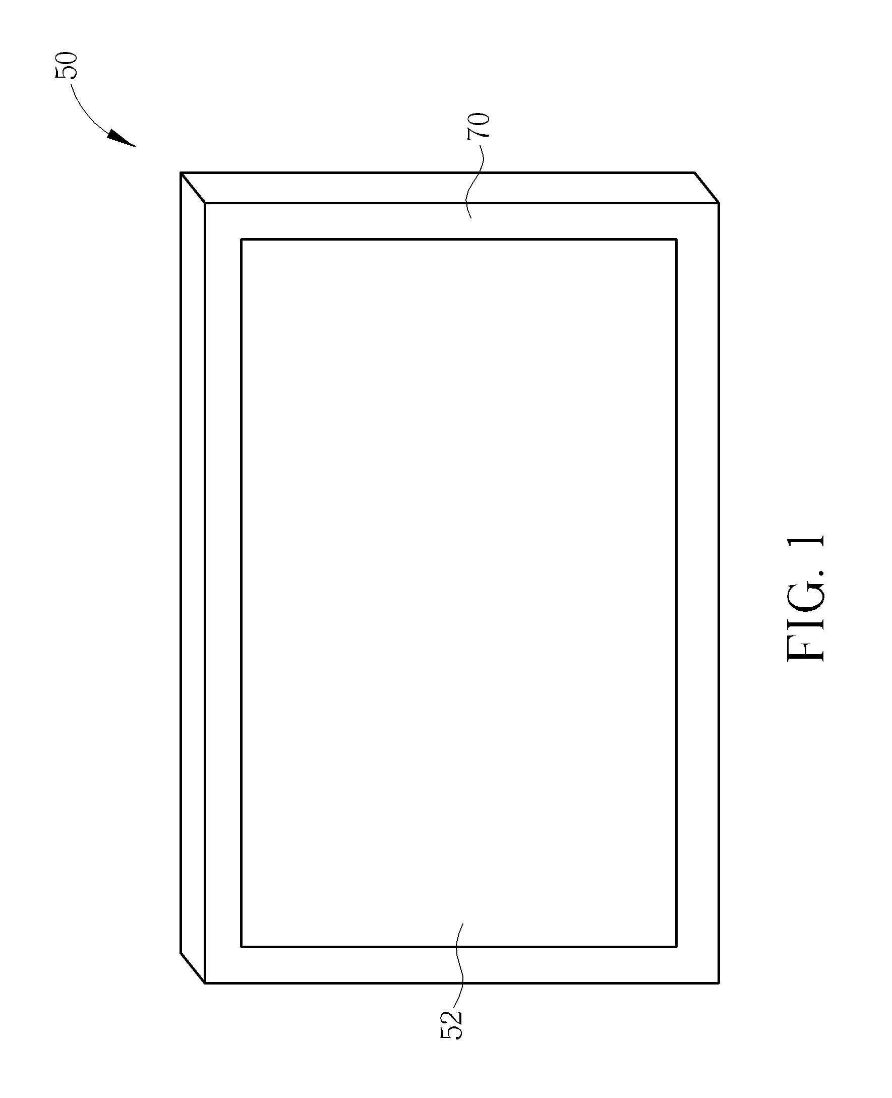
[0020]In the following detailed description of the embodiments, reference is made to the accompanying drawings which form a part hereof, and in which is shown by way of illustration specific embodiments in which the invention may be practiced. In this regard, directional terminology, such as “top,”“bottom,” etc., is used with reference to the orientation of the Figure(s) being described. The components of the present invention can be positioned in a number of different orientations. As such, the directional terminology is used for purposes of illustration and is in no way limiting. On the other hand, the drawings are only schematic and the sizes of components may be exaggerated for clarity. It is to be understood that other embodiments may be utilized and structural changes may be made without departing from the scope of the present invention. Also, it is to be understood that the phraseology and terminology used herein is for the purpose of description and should not be regarded as...


PUM


Abstract

A backlight module includes a light emitting unit for emitting light, a light guide plate disposed on a side of a display panel for guiding the light emitted by the light emitting unit to the display panel, a back cover installed outside the light emitting unit and the light guide plate, and a frame combined with the back cover for accommodating the light emitting unit and the light guide plate with the back cover. The frame includes a first side facing a surface of the light guide plate, and a second side opposite to the first side. The backlight module further includes an optical material layer disposed between the second side of the frame and the display panel for misting and focusing the light refracted from the light guide plate so as to provide uniform and bright light to the display panel.

Description

BACKGROUND OF THE INVENTION[0001]1. Field of the Invention[0002]The present invention relates to a backlight module for providing light to a display panel and a display device therewith, and more particularly, to a backlight module with an optical material layer disposed between a frame and a display panel, and a display device therewith.[0003]2. Description of the Prior Art[0004]With development of technology, a portable electronic device with thin design, less power consumption and portability has been more and more popular in daily life, and a display panel plays an important role therein. Since a liquid crystal display device has advantages of thin shape, less power consumption and non-radiation, it has been widely implemented in the portable electronic device, such as a notebook computer, a personal digital assistant, a cell phone and so on, it has possessed a great market share in the consumer electronic product market. Accordingly, it has been a trend to replace a CRT of a de...

Claims


Application Information

Patent Timeline
Patent Type & Authority Applications(United States)
IPC IPC(8): G09F13/18F21V29/00F21V13/02
CPCG02B6/0085G02B6/0088G02F1/133615
Inventor KUO, YING-TESYU, JYUN-SHENG
Owner WISTRON CORP
Why Eureka
Try Eureka