Silicon carbide substrate, semiconductor device, and soi wafer
a technology of silicon carbide and substrate, which is applied in the direction of polycrystalline material growth, crystal growth process, chemistry apparatus and processes, etc., can solve the problems that silicon carbide used in conventional mechanical parts and the like was not suitable for the material of the substrate, and achieves less high-frequency loss, excellent heat dissipation characteristics, and less high-frequency loss.
- Summary
- Abstract
- Description
- Claims
- Application Information
AI Technical Summary
Benefits of technology
Problems solved by technology
Method used
Image
Examples
embodiment 1
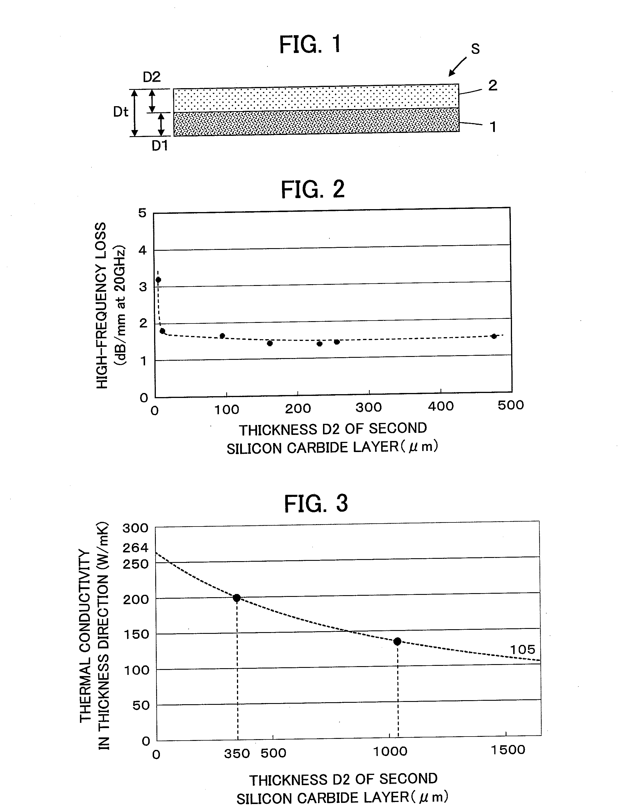
[0027]A silicon carbide substrate S according to Embodiment 1 is shown in FIG. 1. The silicon carbide substrate S is of a two-layer structure including a first silicon carbide layer 1 with a thickness D1 and a second silicon carbide layer 2 with a thickness D2 formed on a surface of the first silicon carbide layer 1. The first and second silicon carbide layers 1 and 2 are each composed of polycrystalline silicon carbide. The second silicon carbide layer 2 has less high-frequency loss than the first silicon carbide layer 1 and the first silicon carbide layer 1 has in the thickness direction a higher thermal conductivity than the second silicon carbide layer 2.
[0028]For example, the first silicon carbide layer 1 has a thermal conductivity of about 260 W / mK, whereas the second silicon carbide layer 2 has a thermal conductivity of about 100 W / mK.
[0029]With regard to the high-frequency loss at a frequency of 20 GHz, the first silicon carbide layer 1 has a value as large as about 50 dB / mm...
embodiment 2
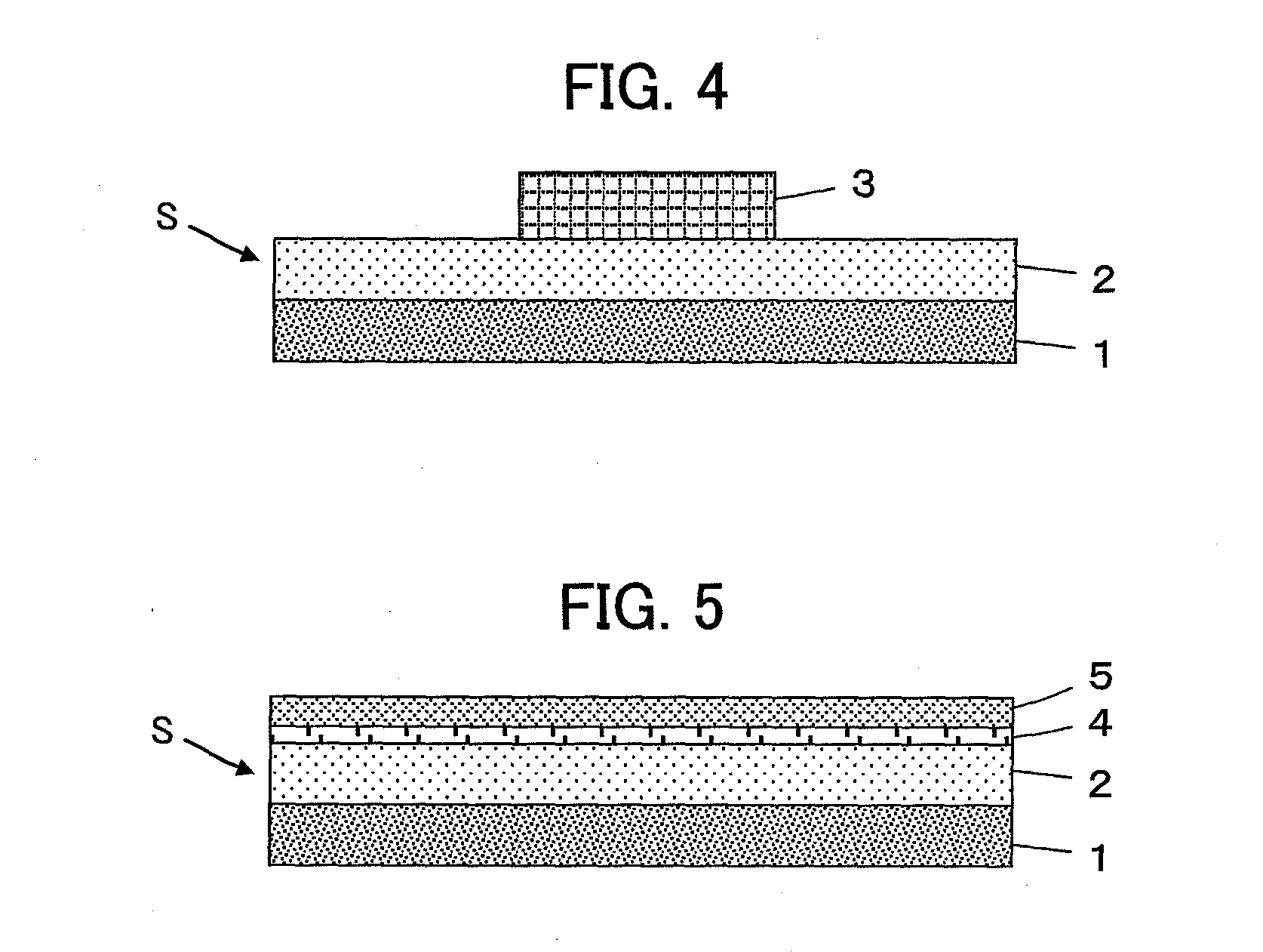
[0050]The configuration of a semiconductor device according to Embodiment 2 is shown in FIG. 4. The semiconductor device is the one having a semiconductor element 3 joined to a surface of the second silicon carbide layer 2 of the silicon carbide substrate S illustrated in Embodiment 1. The semiconductor element 3 is joined to the surface of the second silicon carbide layer 2 by, for example, brazing. It is also possible to form a predetermined conductive pattern on the surface of the second silicon carbide layer 2 and join the semiconductor element 3 onto the conductive pattern using a solder.
[0051]According to the thus configured semiconductor device, the silicon carbide substrate S has a high-frequency loss as small as up to 2 dB / mm at a frequency of 20 GHz on the side of the surface of the second silicon carbide layer 2 on which the semiconductor element 3 is to be mounted, and also has a thermal conductivity of 200 W / mK or more, and therefore enables a highly reliable and stable...
embodiment 3
[0053]The configuration of an SOI (Silicon on Insulator) wafer according to Embodiment 3 is shown in FIG. 5. The SOI wafer is obtained by forming an insulating layer 4 composed of SiO2 or the like on a surface of the second silicon carbide layer 2 of the silicon carbide substrate S illustrated in Embodiment 1 and forming a silicon layer 5 on a surface of the insulating layer 4. The silicon layer 5 is used to form circuit components.
[0054]Also in the SOI wafer, the silicon carbide substrate S has a high-frequency loss as small as up to 2 dB / mm at a frequency of 20 GHz on the surface side of the second silicon carbide layer 2 and also has a thermal conductivity of 200 W / mK or more, and therefore an apparatus capable of a highly reliable and stable operation is realized even when the silicon layer 5 is used to form an element operating in a high-frequency region.
[0055]In addition, since the silicon carbide substrate S has a specific resistance as high as at least 104 Ωcm on the surface...
PUM
 Abstract
Description
Claims
Application Information
 - R&D
- Intellectual Property
- Life Sciences
- Materials
- Tech Scout
- Unparalleled Data Quality
- Higher Quality Content
- 60% Fewer Hallucinations
Browse by: Latest US Patents, China's latest patents, Technical Efficacy Thesaurus, Application Domain, Technology Topic, Popular Technical Reports.
© 2025 PatSnap. All rights reserved.Legal|Privacy policy|Modern Slavery Act Transparency Statement|Sitemap|About US| Contact US: help@patsnap.com


