Etching method and etching device

a technology of etching method and etching device, which is applied in the field of etching, can solve the problems of uneven thickness and slow down the etching process on the surface of the object to be processed, and achieve the effect of preventing the slowdown of the etching speed

Inactive Publication Date: 2012-12-13
SHARP KK
View PDF0 Cites 3 Cited by
  • Summary
  • Abstract
  • Description
  • Claims
  • Application Information

AI Technical Summary

Benefits of technology

[0032]According to the present invention, it becomes possible to allow etching to proceed evenly on the entire surface of the metal film, and a slowdown of the etching speed can be prevented.

Problems solved by technology

If the etching solution is not agitated, it causes a problem of slowing down the etching process on the surface of the object to be processed.
In this case, if the wet etching is continued when the reaction product is formed on the surface of the object to be processed, irregularities are formed on the surface of the object to be processed, resulting in an uneven thickness.

Method used


Image

  • Etching method and etching device
  • Etching method and etching device
  • Etching method and etching device

Examples


Embodiment Construction

[0041]An embodiment of the present invention will be described below in detail with reference to figures.

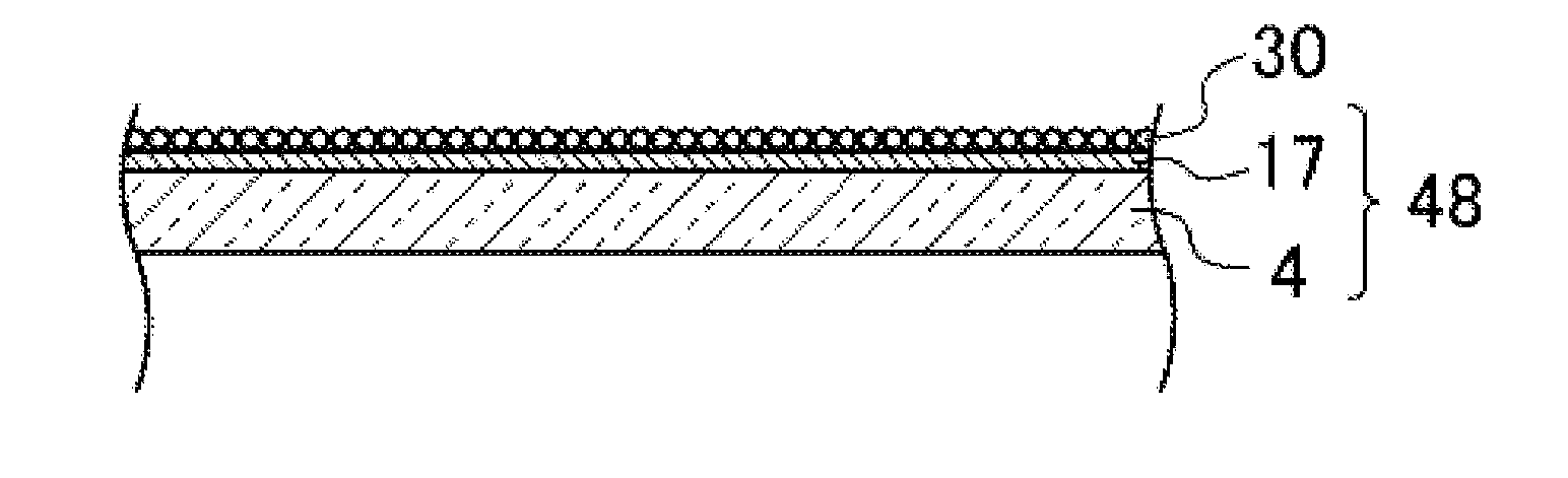
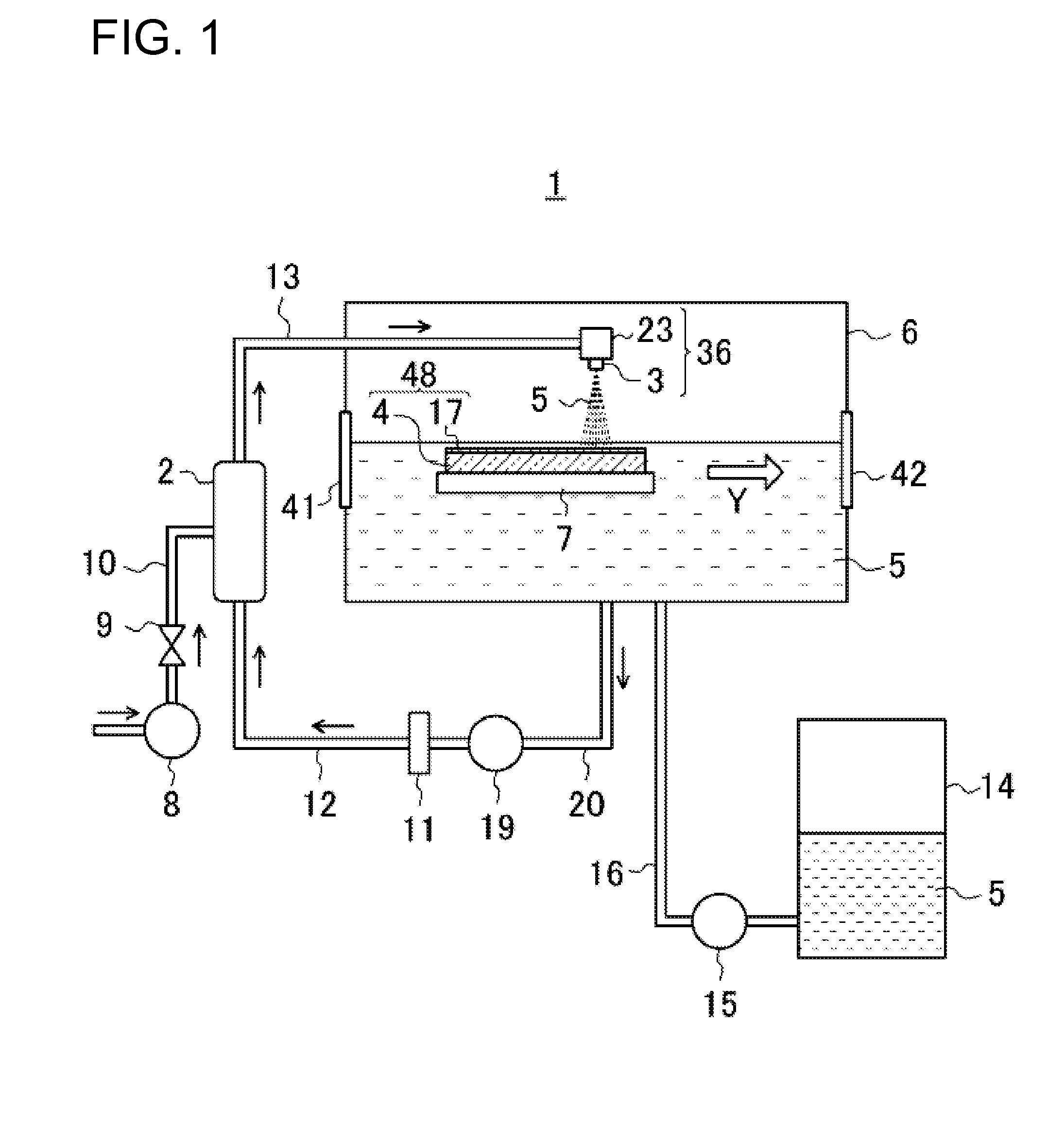
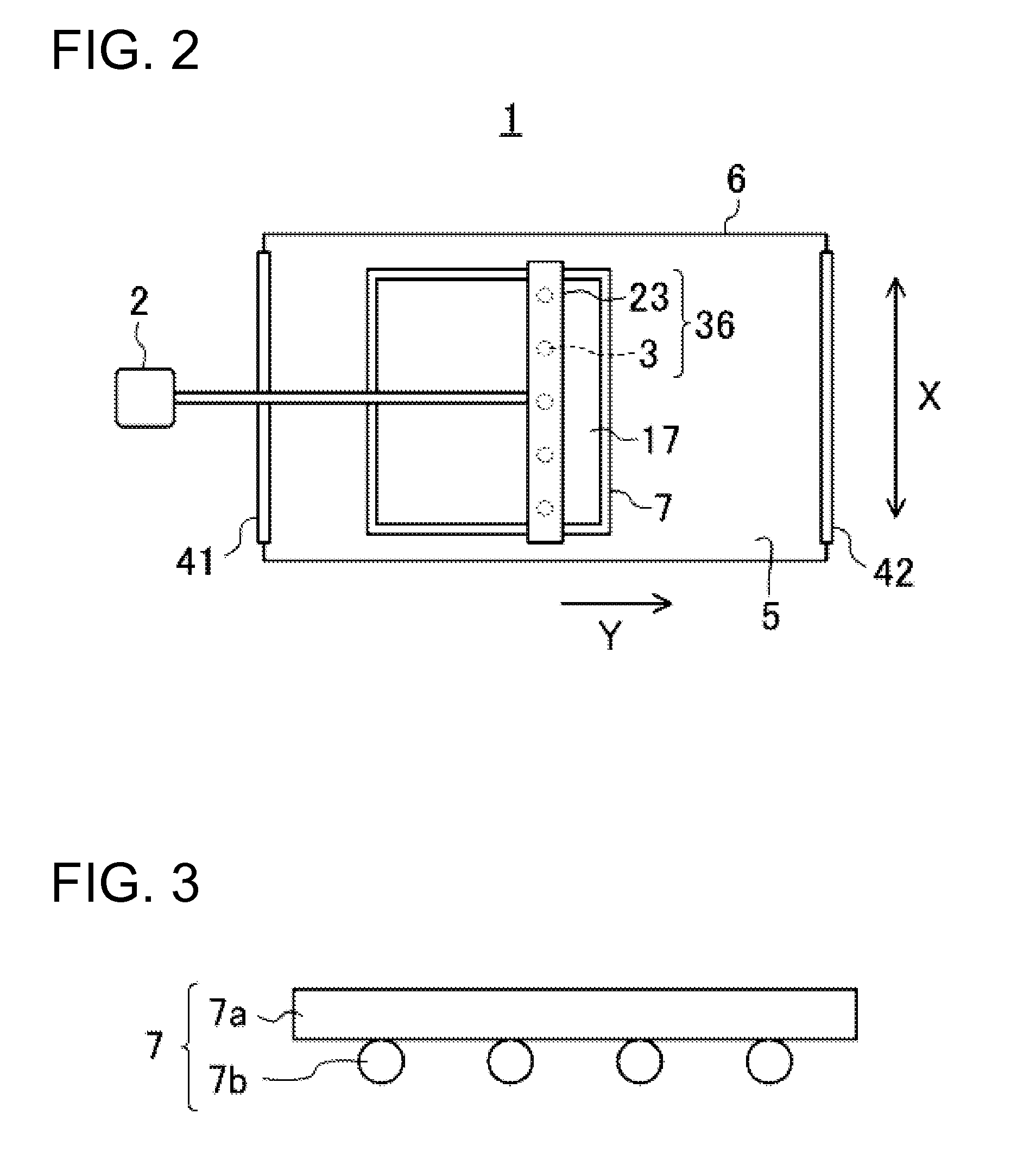
[0042]FIG. 1 is a schematic view showing an overall configuration of an etching device to which an etching method according to an embodiment of the present invention is applied. FIG. 2 is a plan view showing the overall configuration of the etching device to which the etching method according to the embodiment of the present invention is applied. FIG. 3 is an explanatory diagram for a configuration of a holder in the etching device to which the etching method according to the embodiment of the present invention is applied.

[0043]As shown in FIG. 1, an etching device 1 in the present embodiment is provided with an etching solution generation unit (hereinafter referred to as a “generation unit”) 2 that generates an etching solution having gas micro-nano bubbles mixed therein and a nozzle header 36 that is provided with spray nozzles 3 to spray an etching solution 5 that has the micr...


PUM

PropertyMeasurementUnit
diameteraaaaaaaaaa
diameteraaaaaaaaaa
speedaaaaaaaaaa

Abstract

A metal film (17) is etched by having an etching solution (5) sprayed to an object to be processed (48) having the metal film formed on a surface of a substrate (4). The etching solution (5) that contains gas micro-nano bubbles (40) having negative zeta potential is sprayed onto a surface of the metal film (17), removing a metal oxide (30) having positive zeta potential formed thereon.

Description

TECHNICAL FIELD[0001]The present invention relates to an etching method of etching a metal film formed on a substrate, for example, and an etching device.BACKGROUND ART[0002]Conventionally, in a display device such as a liquid crystal display device or an organic EL display device, pixels arranged on a glass substrate in a matrix are controlled by transistors arranged near the pixels, for example. For such transistors, thin film transistors (TFTs) made of an amorphous silicon thin film or a polysilicon thin film have been used to control the pixels.[0003]Photolithography is an indispensable process for forming elements such as the TFTs (thin film transistors) and colored layers of a color filter in a prescribed pattern on a substrate that constitutes a liquid crystal display panel, for example.[0004]After a resist is applied on a semiconductor layer, and a resist pattern is formed by a typical photolithography process, for example, the semiconductor layer exposed from the resist pat...

Claims


Application Information

Patent Timeline
Patent Type & Authority Applications(United States)
IPC IPC(8): C23F1/14B05B1/00
CPCC23F1/08C23F1/14H01L21/67086H01L21/6708H01L21/32134
Inventor TANAKA, JUNICHI
Owner SHARP KK
Why Eureka
Try Eureka