
High-Throughput Semiconductor-Processing Apparatus Equipped with Multiple Dual-Chamber Modules

a semiconductor processing and dual-chamber technology, applied in mechanical control devices, program control, instruments, etc., can solve the problems of wafer handling robots not fully and continuously operating, wafer handling time is getting close to its limit, and the operation of getting shorter

Active Publication Date: 2012-12-06
ASM JAPAN
View PDF7 Cites 370 Cited by
  • Summary
  • Abstract
  • Description
  • Claims
  • Application Information

AI Technical Summary

Benefits of technology

[0022]For purposes of summarizing aspects of the invention and the advantages achieved over the related art, certain objects and advantages of the invention are described in this disclosure. Of course, it is to be understood that not necessarily all such objects or advantages may be achieved in accordance with any particular embodiment of the invention. Thus, for example, those skilled in the art will recognize that the invention may be embodied or carried out in a manner that achieves or optimizes one advantage or group of advantages as taught herein without necessarily achieving other objects or advantages as may be taught or suggested herein.

Problems solved by technology

However, although wafer-handling time (required for unloading / loading a pair of wafers from / to a reaction chamber and moving onto a next reaction chamber) has been getting shorter, due to operational limits of servomotors, friction between wafers (silicon, glass, etc.) and handling materials (ceramics, metal, etc.) for supporting wafers, etc., the wafer-handling time is getting close to its limit, e.g., about 20 seconds when transferring a pair of wafers simultaneously.
Thus, conventionally, the wafer-handling robot is not fully and continuously in operation and waits for the reaction chambers to complete processing.
Thus, in the conventional apparatus, the wafer-handling robot is not fully and continuously in operation and waits for the sub-chambers to complete processing.
Further, because a sub-chamber for precleaning is used, it is difficult to simplify, regulate, and speed up transferring wafers by the wafer-handling robot.

Method used


Image

  • High-Throughput Semiconductor-Processing Apparatus Equipped with Multiple Dual-Chamber Modules
  • High-Throughput Semiconductor-Processing Apparatus Equipped with Multiple Dual-Chamber Modules
  • High-Throughput Semiconductor-Processing Apparatus Equipped with Multiple Dual-Chamber Modules

Examples


Embodiment Construction

[0035]In this disclosure, “gas” may include vaporized solid and / or liquid and may be constituted by a mixture of gases. In this disclosure, the reactive gas, the additive gas, and the hydrogen-containing silicon precursor may be different from each other or mutually exclusive in terms of gas types, i.e., there is no overlap of gas types among these categories. Gases can be supplied in sequence with or without overlap.

[0036]In some embodiments, “film” refers to a layer continuously extending in a direction perpendicular to a thickness direction substantially without pinholes to cover an entire target or concerned surface, or simply a layer covering a target or concerned surface. In some embodiments, “layer” refers to a structure having a certain thickness formed on a surface or a synonym of film. A film or layer may be constituted by a discrete single film or layer having certain characteristics or multiple films or layers, and a boundary between adjacent films or layers may or may n...


PUM

PropertyMeasurementUnit
thicknessaaaaaaaaaa
process timeaaaaaaaaaa

Abstract

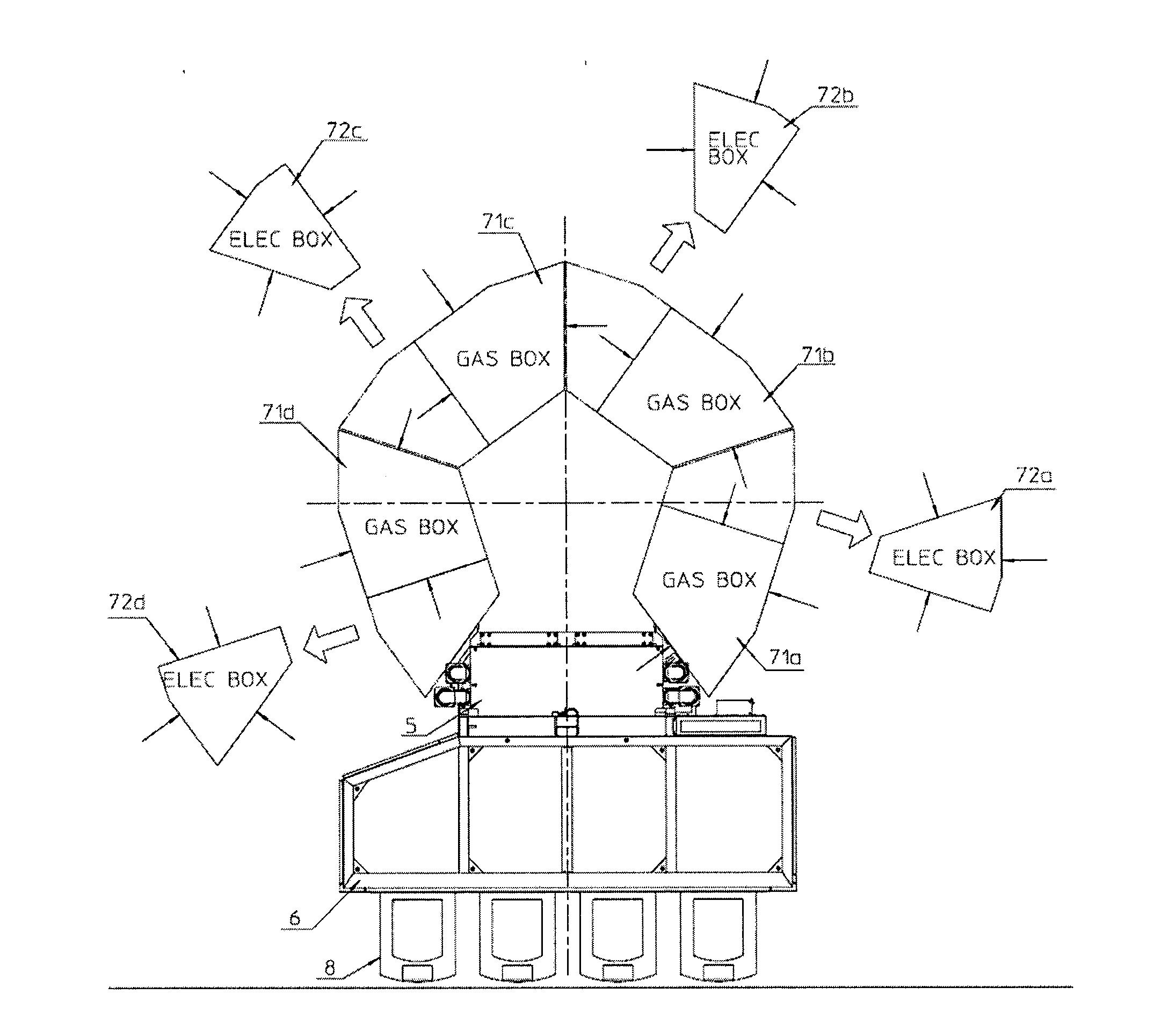
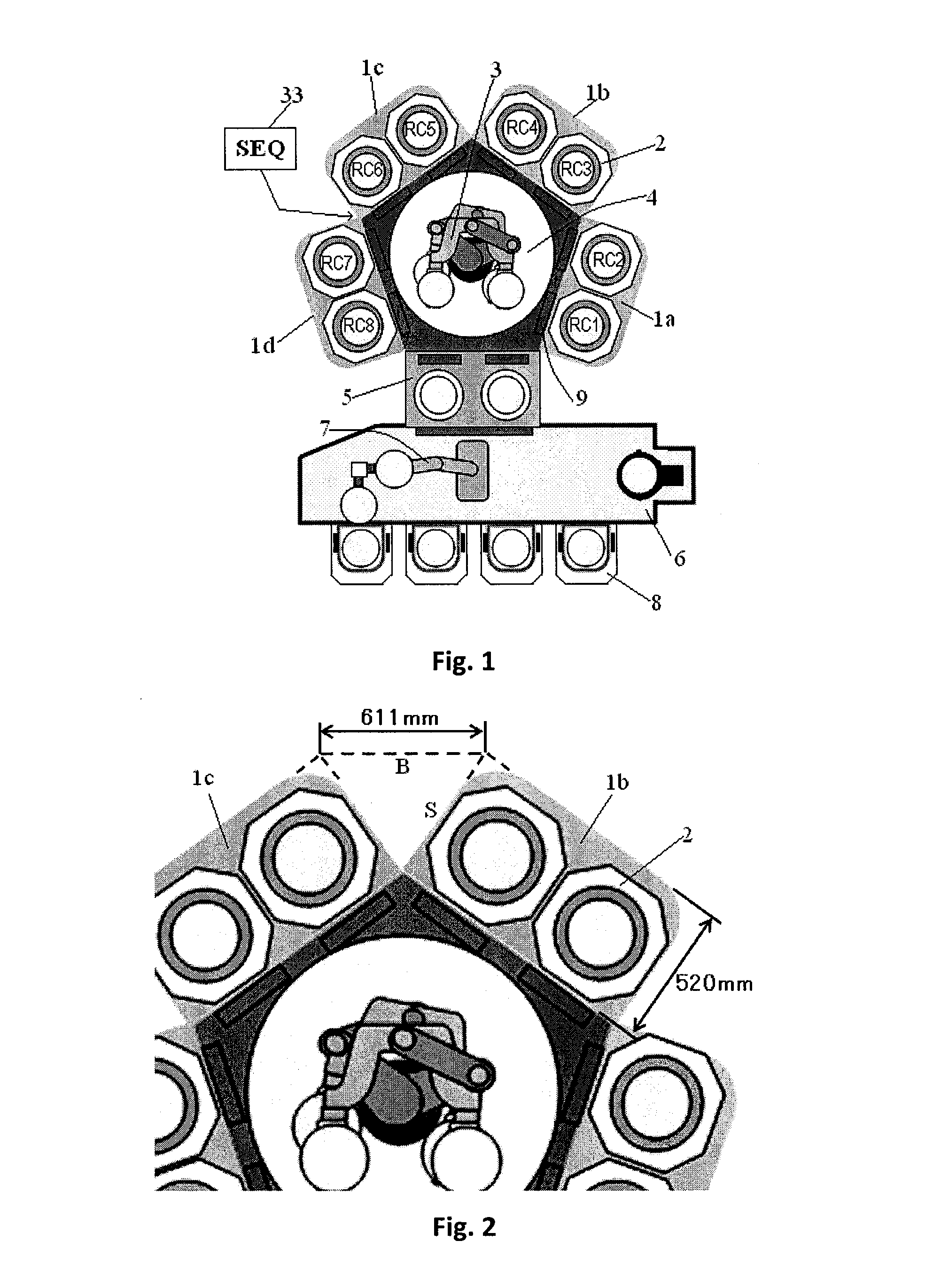
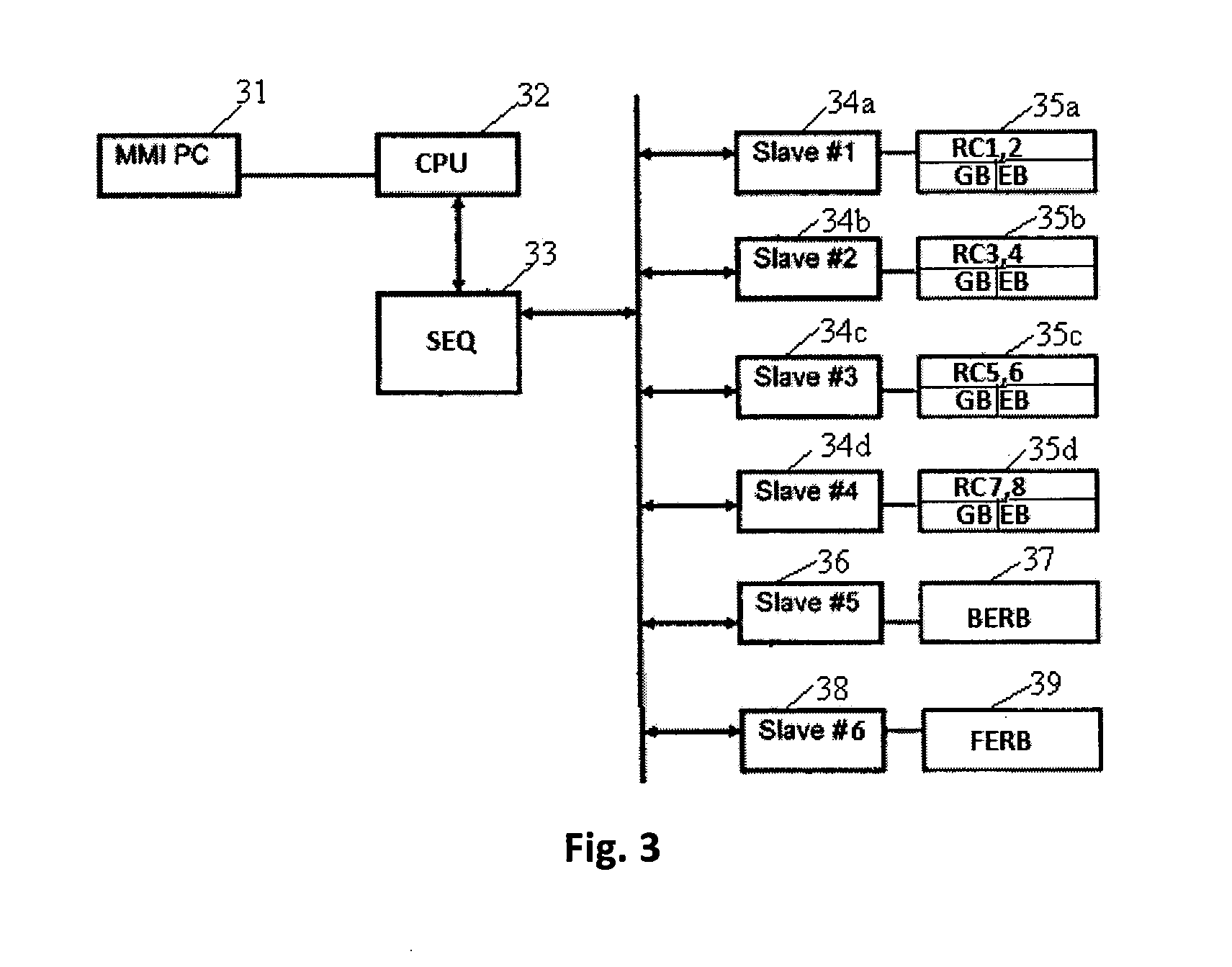
A wafer-processing apparatus includes: eight or ten reactors with identical capacity for processing wafers on the same plane, constituting four or five discrete units, each unit having two reactors arranged side by side with their fronts aligned in a line; a wafer-handling chamber including two wafer-handling robot arms each having at least two end-effectors; a load lock chamber; and a sequencer for performing, using the two wafer-handling robot arms, steps of unloading / loading processed / unprocessed wafers from / to any one of the units, and steps of unloading / loading processed / unprocessed wafers from / to all the other respective units in sequence while the wafers are in the one of the units.

Description

BACKGROUND OF THE INVENTION[0001]1. Field of the Invention[0002]The present invention generally relates to a high-throughput semiconductor-processing apparatus equipped with multiple dual-chamber modules.[0003]2. Description of the Related Art[0004]In the field of CVD apparatuses and etcher apparatuses for treating substrates such as semiconductor wafers, improvement on the productivity or throughput is one important factor. For example, U.S. Pat. No. 6,074,443 teaches a total of four reaction chambers. As shown in FIG. 10, the equipment consists of a preclean chamber 1002 and reaction chambers 1004, 1006 attached to a central chamber 1010 with a transport mechanism 1012, and each processing chamber contains sub-chambers 1002A and B, 1004A and B, and 1006A and B, respectively (the total of reaction sub-chambers is four). Wafers are transferred to wafer cassettes 1008A and B within a load lock 1008. In the apparatus, processing time can be shortened, and productivity can be improved....

Claims


Application Information

Patent Timeline
Patent Type & Authority Applications(United States)
IPC IPC(8): B05C11/10B32B41/00B25J15/00H01L21/683
CPCH01L21/67167H01L21/67742H01L21/6719H01L21/02C23C16/50C23C16/52G05B19/41865G05B2219/32265G05B2219/45031H01L21/67201
Inventor MORI, YUKIHIROYAMAGISHI, TAKAYUKI
Owner ASM JAPAN
Learn More