
Memory address remapping architecture and repairing method thereof

a memory address and memory technology, applied in the field of memory repairing technology, can solve the problems of low repair rate, low yield of memory without being repaired, and inconvenient use of embedded memory and large capacity memory

Inactive Publication Date: 2012-10-18
NATIONAL CHANGHUA UNIVERSITY OF EDUCATION
View PDF9 Cites 10 Cited by
  • Summary
  • Abstract
  • Description
  • Claims
  • Application Information

AI Technical Summary

Benefits of technology

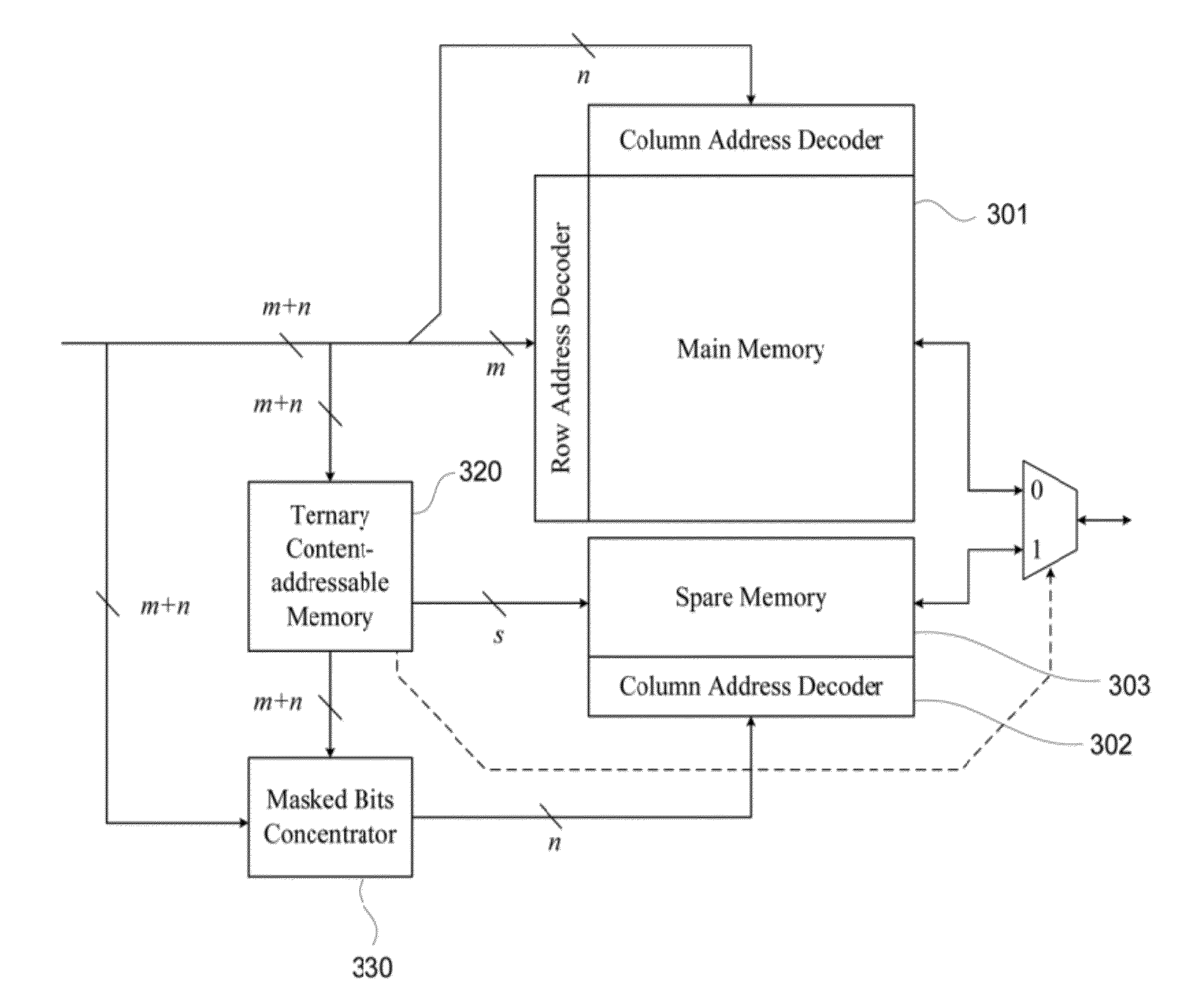
"The patent describes an address remapping method for repairing memory using a ternary content-addressable memory and a masked bits concentrator. This method allows for efficient repair of faults in the memory, including row, column, cluster, and scattered address faults. The use of the hypercube algorithm and the merging of faulty cell addresses with spare memory cells improves the repair rate of the memory. The architecture includes a ternary content-addressable memory, a masked bits concentrator, and a spare memory, which work together to effectively repair the memory."

Problems solved by technology

However, since not only the growth of the memory capacity often breaks the Moore's law, but also the variance increases extremely due to the nanotechnology, the yield of the memory without being repaired is lower than 20%.
Therefore, the technology is not suitable for use in the embedded memory and large capacity memory.
The drawback of the technology is low repair rate.
However, the repairing technology performs poorly to deal with the clustered faults.
As described above, the growth of the memory capacity and variance makes the two-dimensional architecture also perform poorly.
However, the architecture can only deal with array faults on continuous plane, but not to deal with the scattered address fault caused by errors of one or multiple address lines.
First, the architecture cannot be established in an embedded memory effectively, or else the repair rate is low when applying the algorithm in an embedded memory directly.
Second, the architecture still performs poorly to deal with the scattered faults caused by word line defect.
However, the architecture causes some performance impacts on the memory.
On the other hand, the divided spare column and row of the architecture performs poor repair rate to the scattered address faults caused by the address line defects.
Additionally, if no more subcube address is available to cover the faulty Cell address, a failure signal is provided.

Method used


Image

  • Memory address remapping architecture and repairing method thereof
  • Memory address remapping architecture and repairing method thereof
  • Memory address remapping architecture and repairing method thereof

Examples


Embodiment Construction

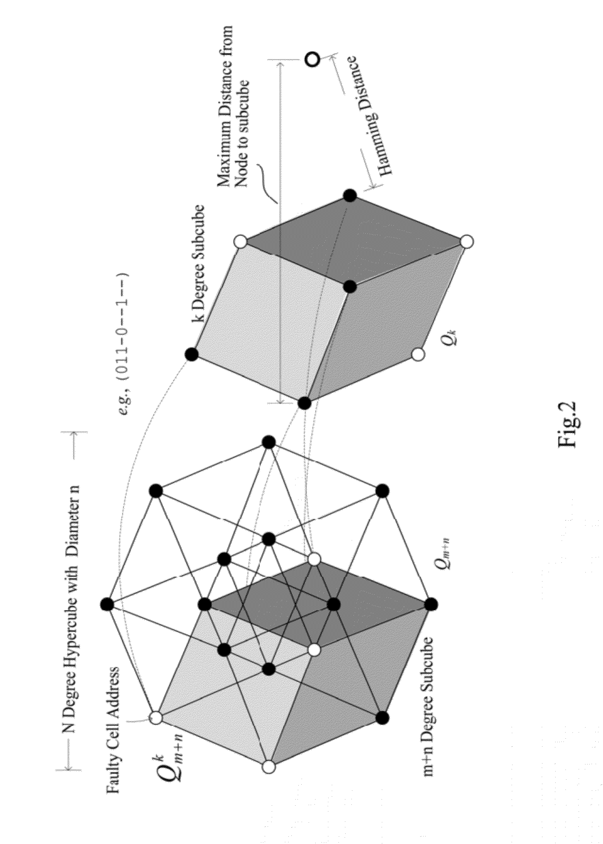
[0029]The disclosure provides a memory address remapping architecture designed by using the hypercube algorithm. The hypercube algorithm applied in repairing memory is introduced as follows.

[0030]Referring to FIG. 2, FIG. 2 is a schematic view of the hypercube algorithm applied in the disclosure for repairing memory. In FIG. 2, an address is defined by a binary code 2n. A N-degree hyper cube Q2nn is indicated as a ternary address Q=(Q2n−1, Q2n−2, . . . Qn, Qn−1, . . . , Q1, Q0), wherein symbol - is applied. In other words, Qi is composed by one of the three symbols (0, 1, -). The symbol - herewith is a union of 0 and 1, instead of the conventional meaning of “don't care”. Additionally, the ternary address Q can also be indicated as a pair of binary value (A, K). Wherein, the masked bit Ki (i=0 . . . 2n−1) is applied to mask the related bits in the address A.

[0031]The concept is that when a faulty cell address is matched with the masked address, the masked address is applied to execu...


PUM


Abstract

A memory address remapping architecture is applied to execute an address remapping method for repairing a main memory. A valid flag and an essential flag in a TCAM corresponding to at least one subcube address in a spare memory are initialized, and the main memory is checked to find out some faulty cell addresses. The Hamming distance between the subcube address and the faulty cell address is calculated, and the faulty cell address is merged into the subcube address by a masked bits concentrator when the Hamming distance is not larger than an address-width degree of the subcube address and the merged number of the subcube address is not larger than a threshold value.

Description

RELATED APPLICATIONS[0001]This application claims priority to Taiwan Patent Application Serial Number 099141225, filed on Nov. 29, 2010. The entire disclosure of the application is hereby incorporated by reference herein.BACKGROUND[0002]1. Technical Field[0003]The present disclosure relates to the memory repairing technology. More particularly, the present disclosure relates to the memory repairing technology that uses a spare memory to cover the faulty cell addresses in a main memory.[0004]2. Description of Related Art[0005]The International Technology Roadmap for Semiconductors (ITRS) from 2001 to 2007 predicts that the embedded memory will occupy 94% of the entire system memory market before 2014. Although the data is modified at 2009, it is still larger than 87%. In recent years, the production value of the memory occupies more than 30% of the entire production value of the semiconductor chips.[0006]However, since not only the growth of the memory capacity often breaks the Moore...

Claims


Application Information

Patent Timeline
Patent Type & Authority Applications(United States)
IPC IPC(8): G06F11/20
CPCG11C29/808G11C29/76
Inventor HUANG, TSUNG-CHU
Owner NATIONAL CHANGHUA UNIVERSITY OF EDUCATION
Learn More