
Wafer boat assembly, loading apparatus comprising such a wafer boat assembly and method for loading a vertical furnace

a technology of wafer boat and loading apparatus, which is applied in the direction of lighting and heating apparatus, cranes, charge manipulation, etc., can solve the problem of a relatively short period of time necessary and achieve the effect of minimizing the dimensions and weight of the second wafer boat, facilitating the loading of semiconductor substrates in a relatively simple way, and reducing the time required for loading the vertical furna

Active Publication Date: 2012-08-23
ASM INTERNATIONAL
View PDF10 Cites 5 Cited by
  • Summary
  • Abstract
  • Description
  • Claims
  • Application Information

AI Technical Summary

Benefits of technology

[0011]By using the proposed loading apparatus containing the proposed wafer boat assembly, a small clearance between wafer edge and cover can be realized and loading of the semiconductor substrates may be automated in a relatively simple way resulting in a relatively short period of time necessary for loading the vertical furnace. Automation of the loading process may be enabled by means of the displacement of a relatively small part of the wafer boat assembly. Handling thereof may be relatively easy due to the minimized dimensions and weight of the second wafer boat part. Consequently, by providing the improved loading apparatus a higher throughput of semiconductor substrates to be processed in a vertical furnace may be obtained.

Problems solved by technology

By using the proposed loading apparatus containing the proposed wafer boat assembly, a small clearance between wafer edge and cover can be realized and loading of the semiconductor substrates may be automated in a relatively simple way resulting in a relatively short period of time necessary for loading the vertical furnace.

Method used


Image

  • Wafer boat assembly, loading apparatus comprising such a wafer boat assembly and method for loading a vertical furnace
  • Wafer boat assembly, loading apparatus comprising such a wafer boat assembly and method for loading a vertical furnace
  • Wafer boat assembly, loading apparatus comprising such a wafer boat assembly and method for loading a vertical furnace

Examples


Embodiment Construction

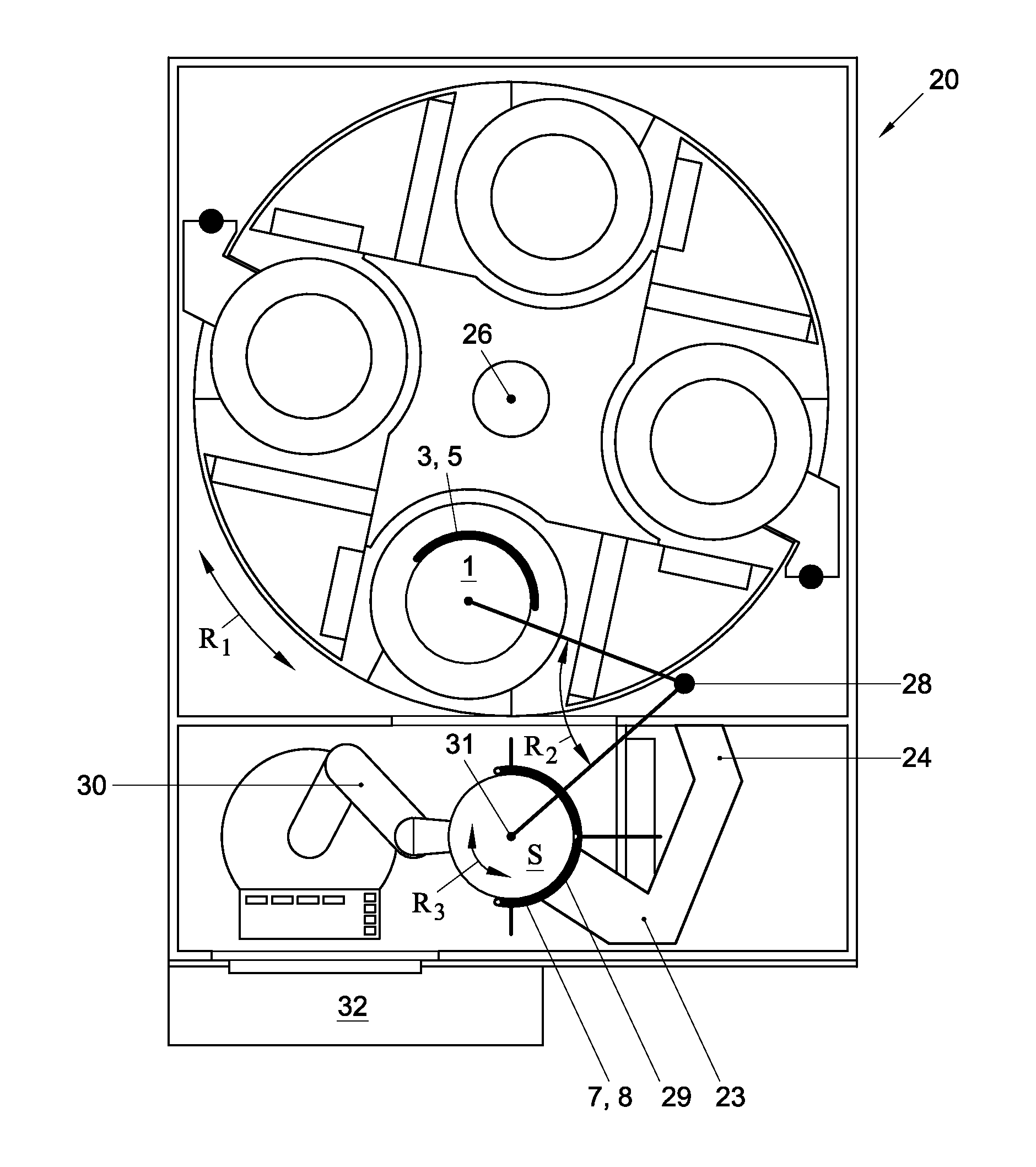
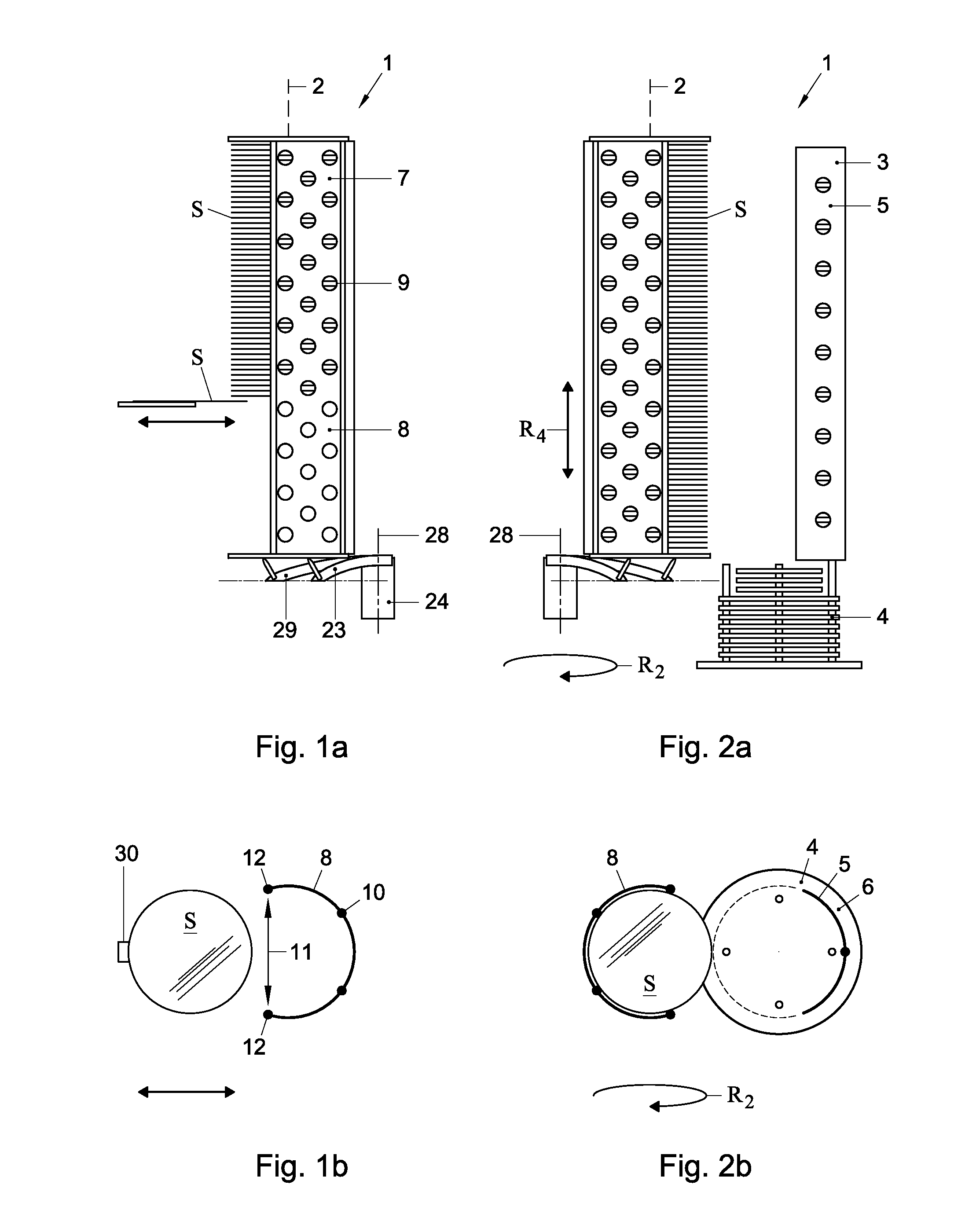
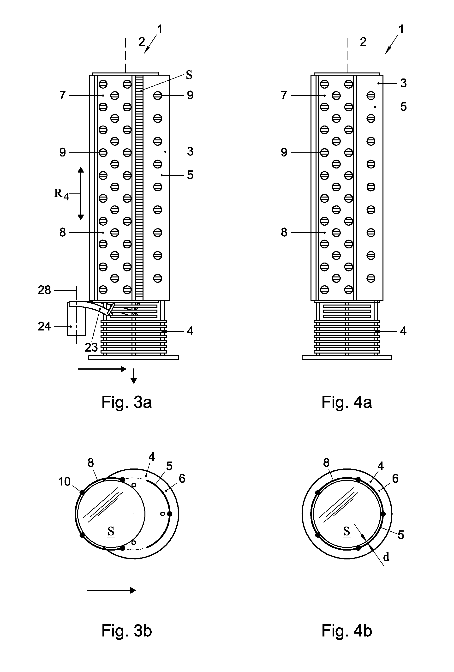
[0025]In FIGS. 1a-4b, an example of a wafer boat assembly 1 for use in a loading apparatus 20 (see FIGS. 5-6) for loading semiconductor substrates S in a vertical furnace is shown in different positions during the loading operation. The wafer boat assembly 1 is configured to be received in a vertical furnace comprising a substantially cylindrical process chamber. During processing of the semiconductor substrates S, a central axis of said process chamber substantially coincides with a central axis 2 of the wafer boat assembly. The vertical furnace may be configured to apply a thin film, for instance by means of a deposition process, on at least one surface of the semiconductor substrates S.

[0026]As is visible in FIGS. 2a, 3a and 4a, the wafer boat assembly 1 may comprise a first wafer boat part 3 comprising a base 4, such as a pedestal, and a first cover part 5. The first cover part 5 is mounted to the base 4 and extends at least partially along an upper perimeter 6 of said base 4 as...


PUM


Abstract

Wafer boat assembly for use in a loading apparatus for loading semiconductor substrates in a vertical furnace configured for batch processing, wherein the wafer boat assembly comprises a wafer boat for holding semiconductor substrates and a cover configured to substantially surround the substrates, wherein the wafer boat assembly is provided witha first wafer boat part comprising a base and a first cover part mounted thereto, said first cover part extending at least partially along a base upper perimeter; anda second wafer boat part comprising a second cover part removably provided on the first wafer boat part and configured to cooperate with the first cover part, said second cover part comprising receiving slots for receiving at least a semiconductor substrate to be processed.

Description

FIELD OF THE INVENTION[0001]The present invention relates to the field of processing of planar thin semiconductor substrates, and more in particular to the loading of semiconductor substrates into a vertical furnace configured for batch processing.BACKGROUND[0002]It is commonly known that semiconductor substrates may be manufactured by means of processes like depositing thin films on surfaces of silicon wafers. Such processes may be carried out in a vertical furnace. Such a vertical furnace is known and typically comprises a process chamber arranged in said furnace such that a central axis of the process chamber substantially coincides, or at least extends in a substantially similar direction, with a central axis of the vertical furnace. Vertical furnaces usually have a load size of 100-150 wafers that are spaced apart such that during processing of the respective wafers the entire surface of each substrate can be subjected to the process. Before processing wafers in a vertical furn...

Claims


Application Information

Patent Timeline
IPC IPC(8): F27D3/00F27B9/38F27D5/00
CPCF27D5/0037F27D3/0084
Inventor DE RIDDER, CHRIS G.M.
Owner ASM INTERNATIONAL
Learn More