Electrical Impedance Imaging
a technology of electrical impedance imaging and apparatus, which is applied in the field of apparatus for electrical impedance imaging, can solve problems such as noise in images caused by reflections, and achieve the effects of high sensitivity, increased current density, and convenient two-dimensional electrical impedance imaging
- Summary
- Abstract
- Description
- Claims
- Application Information
AI Technical Summary
Benefits of technology
Problems solved by technology
Method used
Image
Examples
Embodiment Construction
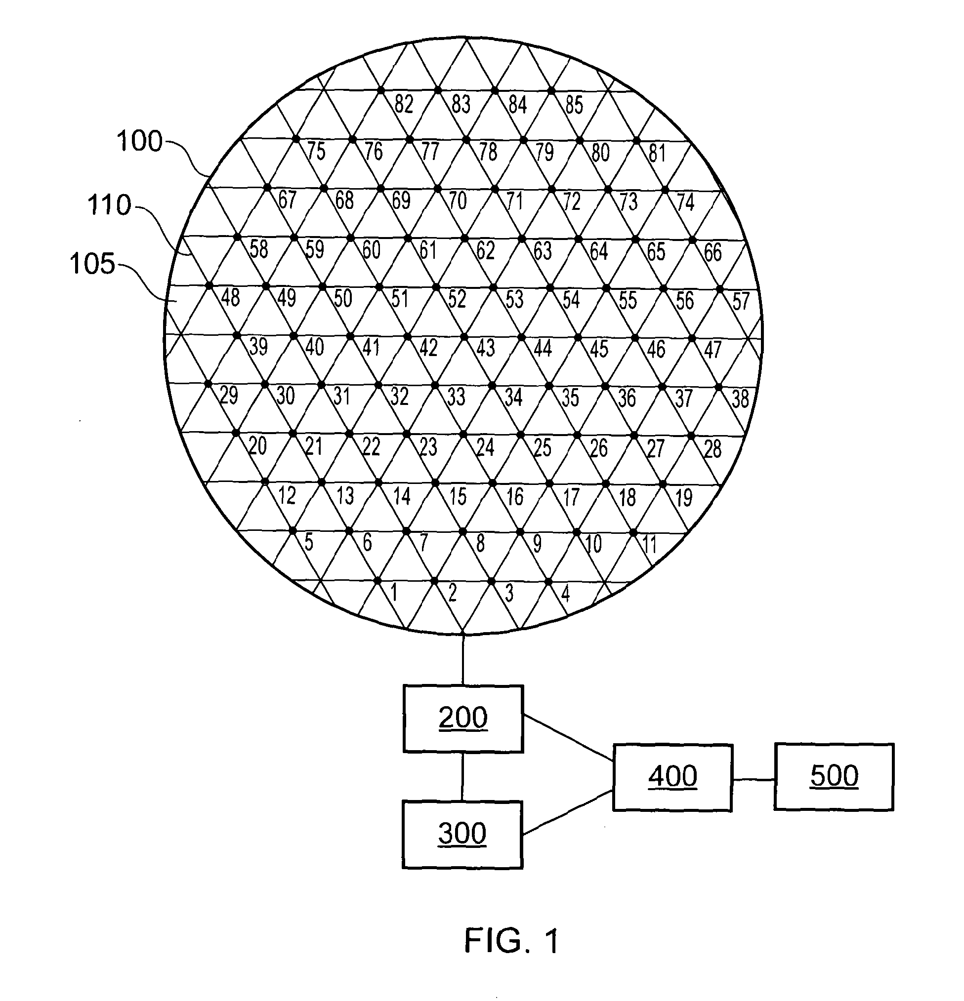
[0061]Referring to FIG. 1, there is a circular carrier 100 which is electrically non-conductive and which may be made, for example, of a plastic material. Electrodes 1-85 are deployed across a flat surface 105 of the electrode carrier 100 and are preferably recessed in the electrode carrier 100 so that they do not make physical contact with an object placed on the electrode carrier 100. There are eighty five electrodes, each denoted in FIG. 1 by a dot, and for ease of reference indicated by reference numerals 1 to 85 respectively. The electrodes 1-85 are arranged equidistant in a triangular matrix, such that the electrodes 1-85 are located at corners of equilateral triangles arranged in a continuum. In such an arrangement, each electrode 1-85, except those adjacent the boundary of the arrangement, has six nearest neighbour electrodes 1-85 which are arranged in a hexagon. For example, the nearest neighbours to electrode 7 are electrodes 1, 2, 6, 8, 14, 15. In FIG. 1, the electrodes 1...
PUM
 Abstract
Description
Claims
Application Information
 - R&D
- Intellectual Property
- Life Sciences
- Materials
- Tech Scout
- Unparalleled Data Quality
- Higher Quality Content
- 60% Fewer Hallucinations
Browse by: Latest US Patents, China's latest patents, Technical Efficacy Thesaurus, Application Domain, Technology Topic, Popular Technical Reports.
© 2025 PatSnap. All rights reserved.Legal|Privacy policy|Modern Slavery Act Transparency Statement|Sitemap|About US| Contact US: help@patsnap.com


