Optical element, light source device, and projection display device
a technology of light source and optical element, which is applied in the direction of instruments, lighting and heating apparatus, planar/plate-like light guides, etc., can solve the problems of increasing the etendue of the light source itself, the overall size of the light-emitting area of the light source, etc., and achieve the effect of reducing the etendue of the light from the optical elemen
- Summary
- Abstract
- Description
- Claims
- Application Information
AI Technical Summary
Benefits of technology
Problems solved by technology
Method used
Image
Examples
first embodiment
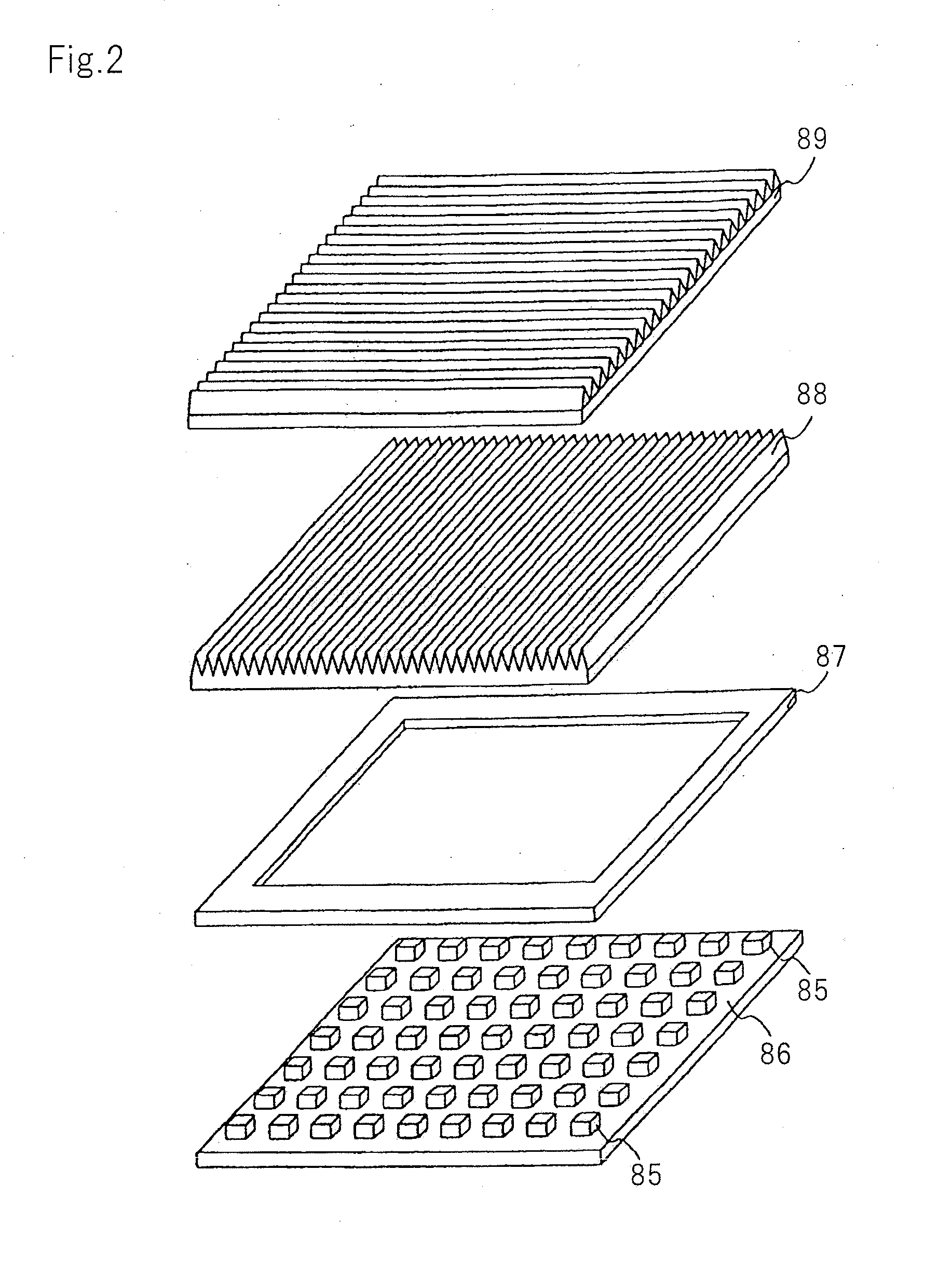
[0066]FIG. 3 is a schematic perspective view showing a configuration of a light source device according to a first embodiment. FIG. 4 is an explanatory sectional view showing behavior of light in the light source device according to the present invention. In the light source device, individual layers actually have a very large thickness, and there is a large difference in thickness among the layers. It is therefore difficult to draw the layers in accurate scale and proportion. Thus, in the drawings, the layers are not drawn in actual proportion, and hence are schematically shown.
[0067]As shown in FIGS. 3 and 4, light source device 50 according to the present embodiment includes a plurality of light-emitting elements 1 (1a to 1n) and optical element 51 into which lights output from light-emitting elements 1 enter. Optical element 51 includes light guide body 2 into which the lights output from light-emitting elements 1 enter, and directional control layer 3 for emitting output light ...
second embodiment
[0109]FIG. 11 is a perspective view showing a directional control layer included in a light source device according to a second embodiment. As shown in FIG. 11, in directional control layer 18 according to the second embodiment, carrier generation layer 16, plasmon excitation layer 8, and wave vector conversion layer 17 made of a photonic crystal are stacked in order on light guide body 2.
[0110]In directional control layer 18 according to the second embodiment, wave vector conversion layer 17 also functions as high dielectric constant layer 9 of the first embodiment, and carrier generation layer 16 also functions as low dielectric constant layer 7 of the first embodiment. Thus, to generate plasmon coupling at plasmon excitation layer 8, a dielectric constant of wave vector conversion layer 17 located adjacent to the exit side interface of plasmon excitation layer 8 is set higher than that of carrier generation layer 16 located adjacent to the incident side interface of plasmon excit...
third embodiment
[0112]FIG. 12 is a perspective view showing a directional control layer included in a light source device according to a third embodiment. As shown in FIG. 12, in directional control layer 19 according to the third embodiment, carrier generation layer 6, low dielectric constant layer 7, plasmon excitation layer 8, and wave vector conversion layer 17 made of a photonic crystal are stacked in order on light guide body 2.
[0113]In directional control layer 19 according to the third embodiment, wave vector conversion layer 17 also functions as high dielectric constant layer 9 of the first embodiment. Thus, to generate plasmon coupling at plasmon excitation layer 8, the dielectric constant of wave vector conversion layer 17 is set higher than that of low dielectric constant layer 7. However, even when the dielectric constant of wave vector conversion layer 17 is lower than that of low dielectric constant layer 7, directional control layer 19 operates as long as the real part of the effect...
PUM
| Property | Measurement | Unit |
|---|---|---|
| thickness | aaaaa | aaaaa |
| thickness | aaaaa | aaaaa |
| thickness | aaaaa | aaaaa |
Abstract
Description
Claims
Application Information
 - R&D
- Intellectual Property
- Life Sciences
- Materials
- Tech Scout
- Unparalleled Data Quality
- Higher Quality Content
- 60% Fewer Hallucinations
Browse by: Latest US Patents, China's latest patents, Technical Efficacy Thesaurus, Application Domain, Technology Topic, Popular Technical Reports.
© 2025 PatSnap. All rights reserved.Legal|Privacy policy|Modern Slavery Act Transparency Statement|Sitemap|About US| Contact US: help@patsnap.com


