Manufacturing method of semiconductor device
a manufacturing method and semiconductor technology, applied in the field of semiconductor devices, can solve the problem of negative shift of the threshold voltage of the transistor, and achieve the effect of favorable electric characteristics and less likely to chang
- Summary
- Abstract
- Description
- Claims
- Application Information
AI Technical Summary
Benefits of technology
Problems solved by technology
Method used
Image
Examples
embodiment mode 1
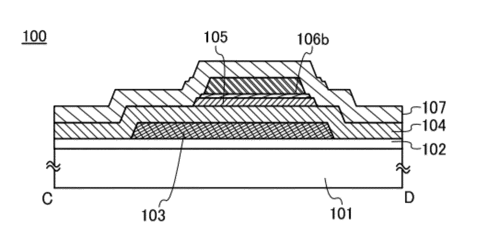
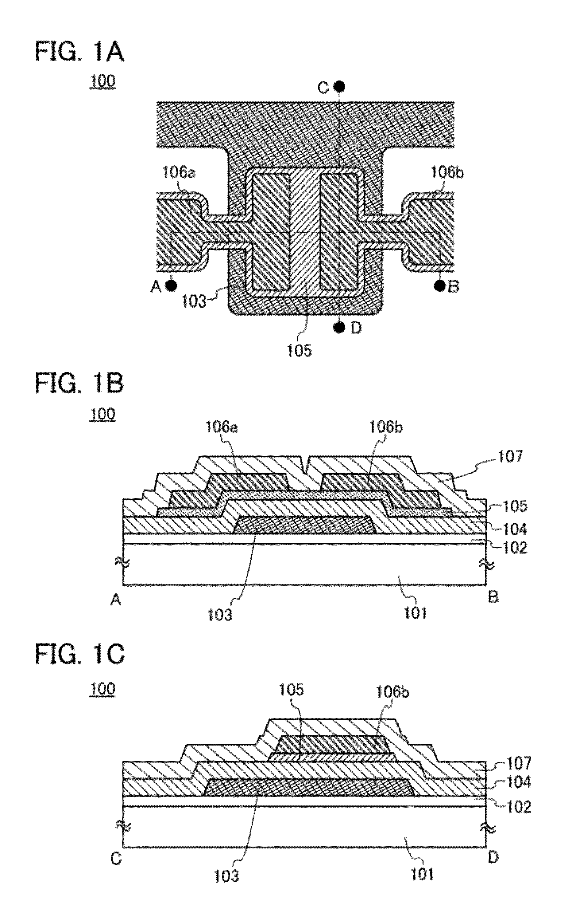
[0057]In this embodiment mode, a transistor and a manufacturing method thereof, each of which is one embodiment of the present invention, are described with reference to FIGS. 1A to 1C, FIGS. 2A to 2C, FIGS. 3A to 3C, FIGS. 4A to 4D, FIGS. 5A and 5B, FIGS. 6A and 6B, and FIGS. 7A and 7B.
[0058]FIG. 1A is a top view illustrating a structure of a transistor 100 which is one embodiment of the present invention. FIG. 1B is a cross-sectional view taken along dashed-dotted line A-B in FIG. 1A, and FIG. 1C is a cross-sectional view taken along dashed-dotted line C-D in FIG. 1A. Note that in FIG. 1A, a base insulating film 102, a gate insulating film 104, and a protective insulating film 107 are not shown for simplicity.
[0059]In FIGS. 1B and 1C, the transistor 100 includes a substrate 101, the base insulating film 102 provided over the substrate 101, a gate electrode 103 provided over the base insulating film 102, the gate insulating film 104 provided over the gate electrode 103, an oxide se...
embodiment mode 2
[0188]In this embodiment mode, a mode in which the oxide semiconductor film 105 in each of the transistor 100, the transistor 200, and the transistor 310 in Embodiment Mode 1 is an oxide semiconductor film including a crystalline region is described. The mode can be obtained by a manufacturing process partly different from the manufacturing process described in Embodiment Mode 1. Note that the same reference numerals are used for the same parts as those in Embodiment Mode 1, and specific description of the parts with the same reference numerals is omitted here.
[0189]The oxide semiconductor film including a crystalline region described in this embodiment is non-single-crystal. Specifically, oxide semiconductor film includes a crystalline region having a triangular, hexagonal, regular triangular, or regular hexagonal atomic arrangement when seen from the direction perpendicular to the a-b plane and in which metal atoms are arranged in a layered manner or metal atoms and oxygen atoms a...
embodiment mode 3
[0206]In this embodiment mode, verification results on how easily oxygen deficiency is produced at a top surface and a side surface of an oxide semiconductor film included in a transistor manufactured according to any of the manufacturing methods described in Embodiment Modes 1 and 2, obtained through calculation using the following models, are described. Note that the CAAC oxide semiconductor described in Embodiment Mode 2 is complicated to be used as a model of calculation due to having a plurality of crystal planes on one side surface. Therefore, calculation is conducted here using a ZnO single crystal that has a wurtzite structure having c-axis alignment. As crystal models, the (001) plane, the (100) plane, and the (110) plane obtained by cutting the crystal structure along planes parallel to the c-axis and a plane perpendicular to the c-axis as shown in FIG. 25 are used.
[0207]The calculation results in this embodiment mode are obtained in the following manner: after making the ...
PUM
 Abstract
Description
Claims
Application Information
 - R&D
- Intellectual Property
- Life Sciences
- Materials
- Tech Scout
- Unparalleled Data Quality
- Higher Quality Content
- 60% Fewer Hallucinations
Browse by: Latest US Patents, China's latest patents, Technical Efficacy Thesaurus, Application Domain, Technology Topic, Popular Technical Reports.
© 2025 PatSnap. All rights reserved.Legal|Privacy policy|Modern Slavery Act Transparency Statement|Sitemap|About US| Contact US: help@patsnap.com


