Thin film transistor array substrate and manufacturing method thereof

a technology of thin film transistors and array substrates, which is applied in the direction of semiconductor/solid-state device manufacturing, semiconductor devices, electrical devices, etc., can solve the problems of increasing the power load of lcd panels, and achieve the effects of reducing power loading, simple structure, and fewer processing steps

Active Publication Date: 2012-06-28
AU OPTRONICS CORP
View PDF4 Cites 2 Cited by
  • Summary
  • Abstract
  • Description
  • Claims
  • Application Information

AI Technical Summary

Benefits of technology

[0030]Based on the above, a thin film transistor array substrate is proposed in present invention. The proposed thin film transistor array substrate is with few processing steps and a simple structure, wherein merely two patterned metal layers are required. And a patterned planarization layer is adopted to separate the two patterned metal layers from each other and thereby reduce the power loading. In addition, the patterned planarization layer has slots to form height differences to separate scan lines from common electrodes to further reduce the power loading.

Problems solved by technology

However, the storage capacitor electrode massively overlapping the scan signal transmission line or data line would cause the power load of LCD panel increase.

Method used


Image

  • Thin film transistor array substrate and manufacturing method thereof
  • Thin film transistor array substrate and manufacturing method thereof
  • Thin film transistor array substrate and manufacturing method thereof

Examples


Embodiment Construction

[0037]Reference will now be made in detail to the present preferred embodiments of the invention, examples of which are illustrated in the accompanying drawings. Wherever possible, the same reference numbers are used in the drawings and the description to refer to the same or like parts.

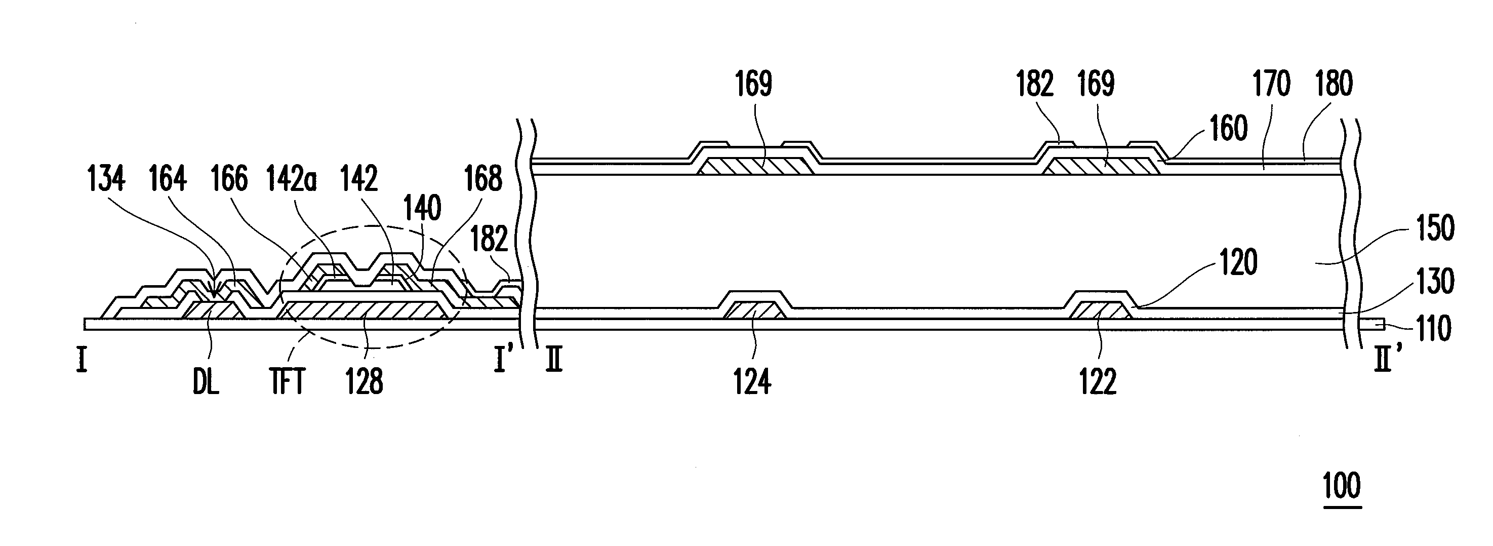
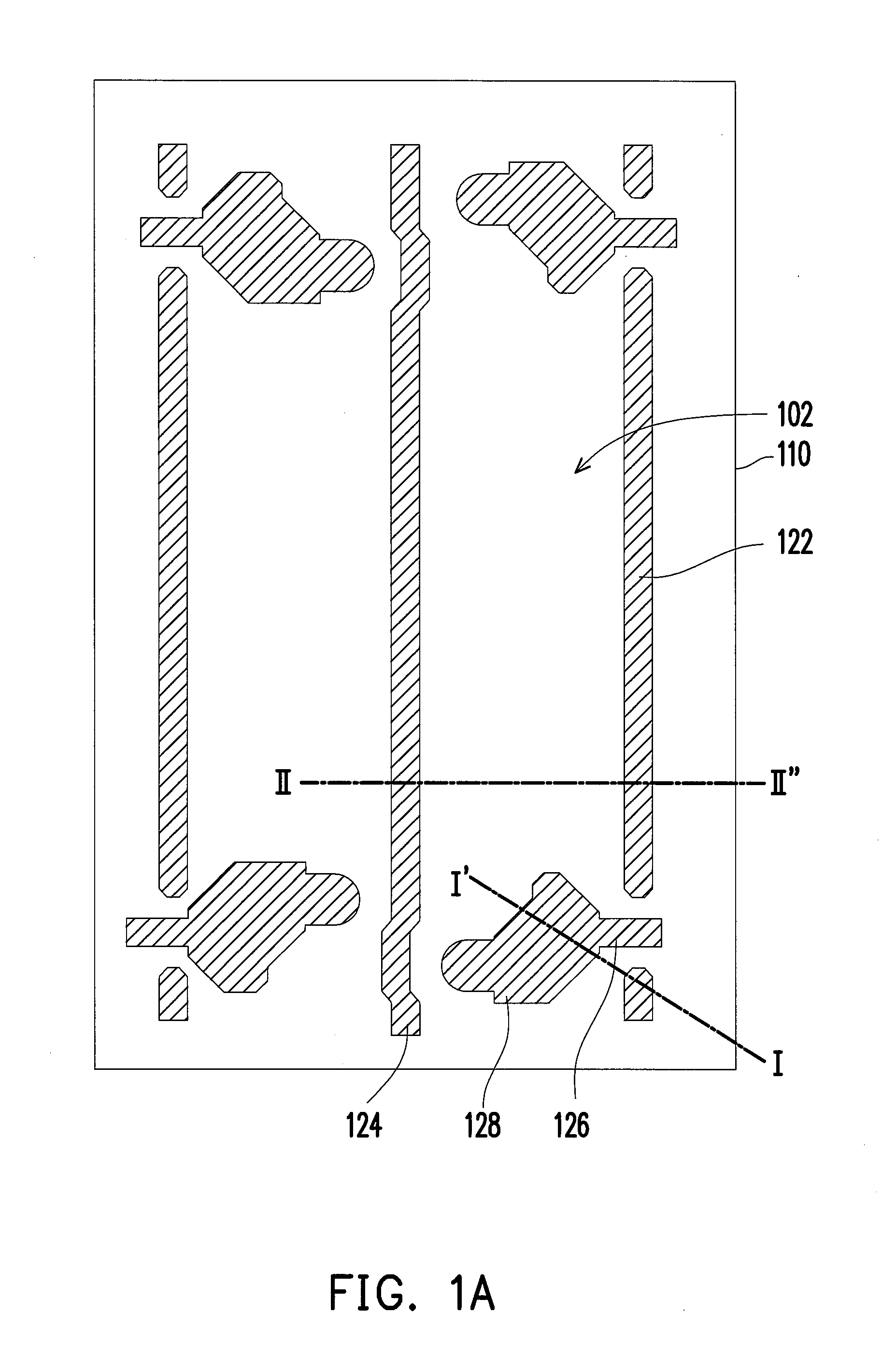
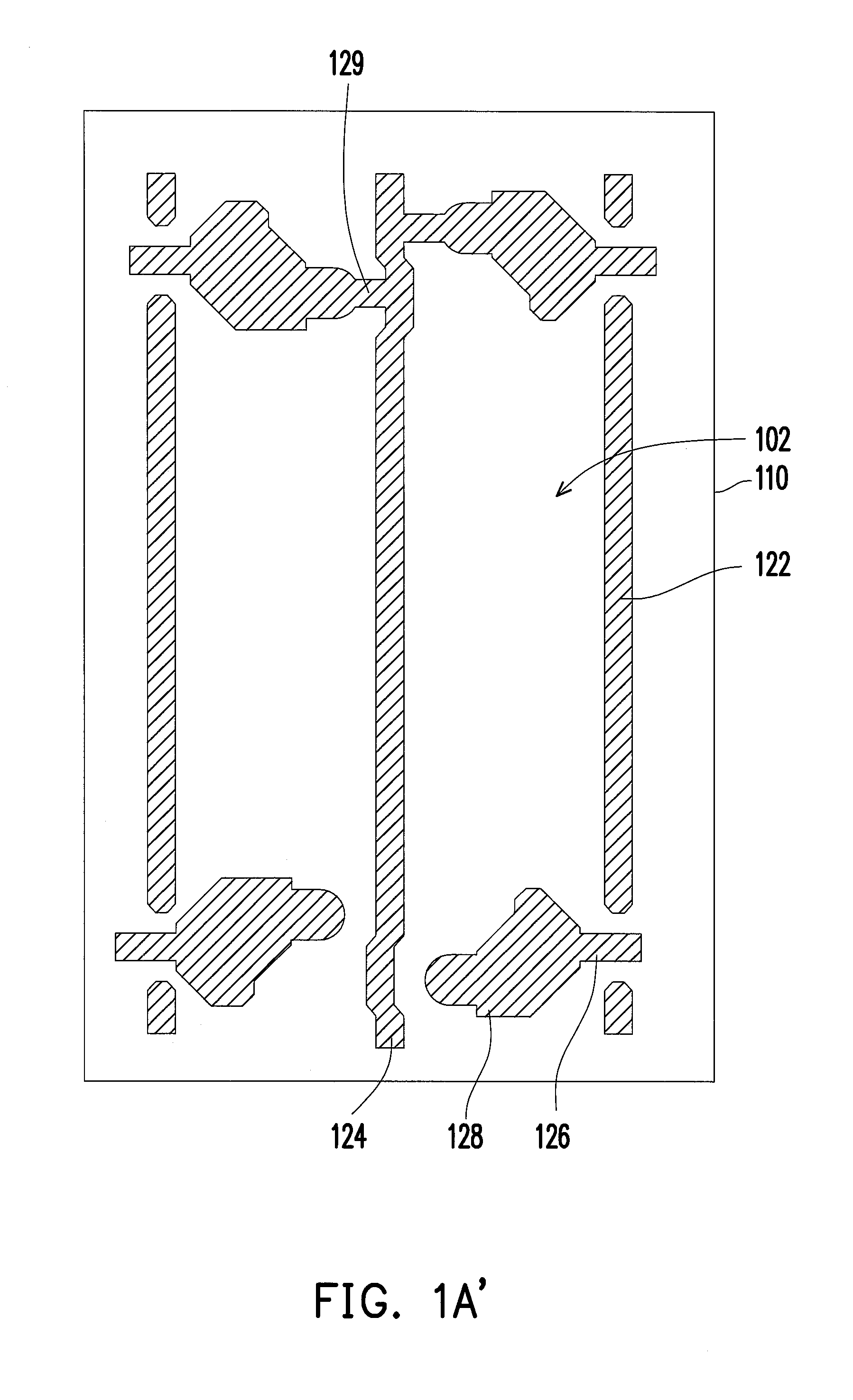
[0038]FIGS. 1A-1G sequentially illustrate the process flow of a thin film transistor array substrate according to an embodiment of present invention. FIGS. 2A-2G are cross section views along the line I-I′ and the line II-II′ of FIGS. 1A-1G.

[0039]First, as shown in FIG. 1A and FIG. 2A, a substrate 110 is provided and a first photolithographic process is done to form a patterned first metal layer 120 on the substrate 110. The patterned first metal layer 120 comprises a plurality of quasi-data lines 122 which are parallel to each other and a plurality of scan signal transmission lines 124 which are parallel to the quasi-data lines 122, wherein one scan signal transmission line 124 is disposed between e...


PUM


Abstract

A thin film transistor (TFT) array substrate with few processing steps and simple structure is provided, wherein merely two patterned metal layers are required and a patterned planarization layer is adopted to separate the two patterned metal layers from each other and thereby reduce power loading. In addition, the patterned planarization layer has slots to form height differences so as to separate scan lines from common electrodes to further reduce the power loading.

Description

CROSS-REFERENCE TO RELATED APPLICATION[0001]This application claims the priority benefit of Taiwan application serial no. 99146144, filed Dec. 27, 2010. The entirety of the above-mentioned patent application is hereby incorporated by reference herein and made a part of this specification.BACKGROUND OF THE INVENTION[0002]1. Field of the Invention[0003]The present invention generally relates to active device array substrate and manufacturing method thereof. More particularly, the present invention relates to a thin film transistor (TFT) array substrate and manufacturing method thereof.[0004]2. Description of Related Art[0005]In general, a liquid crystal display panel (LCD panel) is mainly comprised of an active device array substrate, an opposite substrate, and a liquid crystal layer sandwiched between the active device array substrate and the opposite substrate. The active device array substrate has a display region and a non-display region. A plurality of pixel units are arranged on...

Claims


Application Information

Patent Timeline
Patent Type & Authority Applications(United States)
IPC IPC(8): H01L33/16
CPCH01L27/124H01L29/41733H01L27/1248
Inventor YEN, ZE-YUCHANG, KE-CHIHHUANG, KUO-YULIN, EN-YUNG
Owner AU OPTRONICS CORP
Why Eureka
Try Eureka