Method for Defining an Electronically Conductive Metal Structure on a Three-Dimensional Element and a Device Made From the Method

a three-dimensional element and metal structure technology, applied in the field of photolithographic technologies, can solve the problems of introducing a potential for lower yield and challenging the definition of electrical conductive metal traces or electrodes on the surface of the structur

Inactive Publication Date: 2012-04-19
PFG IP +1
View PDF4 Cites 8 Cited by
  • Summary
  • Abstract
  • Description
  • Claims
  • Application Information

AI Technical Summary

Benefits of technology

The invention is a method for creating electrically conductive metal structures on the surface of a three-dimensional element, such as a glass microsphere or shell resonator. The method uses a maskless photolithographic process and a specific type of laser to create the metal structure. The substrate can be a silicon layer or a glass shell resonator. The metal layer is deposited on the surface of the three-dimensional element and then a photoresist layer is applied. The photoresist layer is exposed to a pattern and developed to create the metal structure. The invention allows for precise placement of metal structures on the surface of three-dimensional elements, which can be useful in various applications such as sensors or electronics.

Problems solved by technology

Because shell resonator structures have relatively small feature sizes and radial and non-planar surfaces, defining the electrical conductive metal traces or electrodes on the surface of the structure is challenging.
Prior art attempts include defining metal traces on a flat glass layer in a Pyrex-Si wafer stack prior to forming the resonator structures in a high temperature thermal process but difficulty in devising a metal stack with sufficient ductility to permit plastic deformation concurrent with the formation of the glass shell structure requires complex, costly, multiple plating steps, each of which introduces a potential for lower yields.

Method used


Image

  • Method for Defining an Electronically Conductive Metal Structure on a Three-Dimensional Element and a Device Made From the Method
  • Method for Defining an Electronically Conductive Metal Structure on a Three-Dimensional Element and a Device Made From the Method

Examples


Embodiment Construction

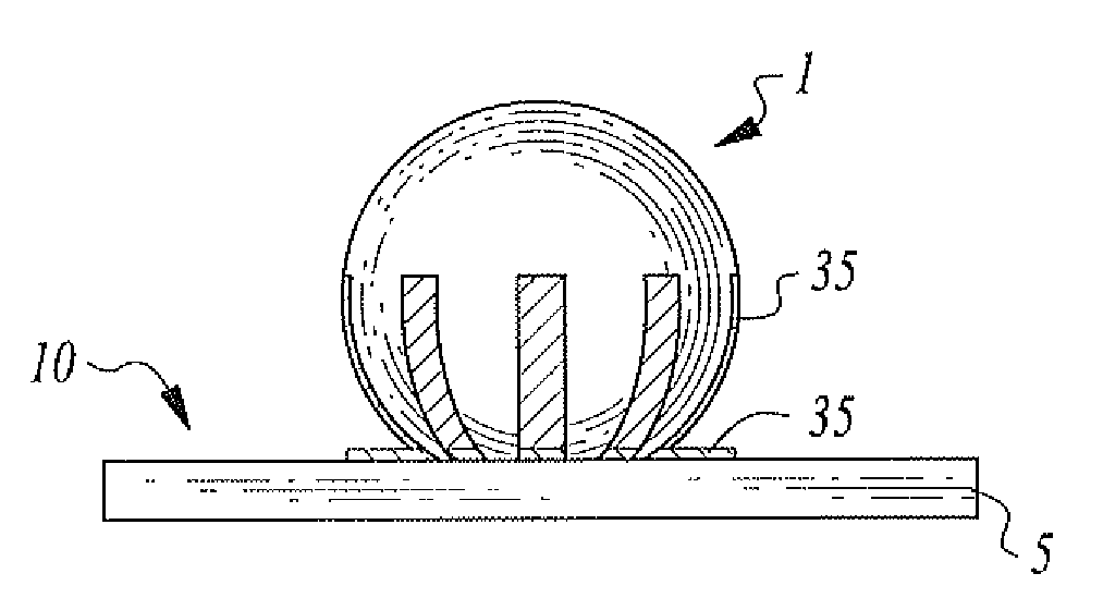
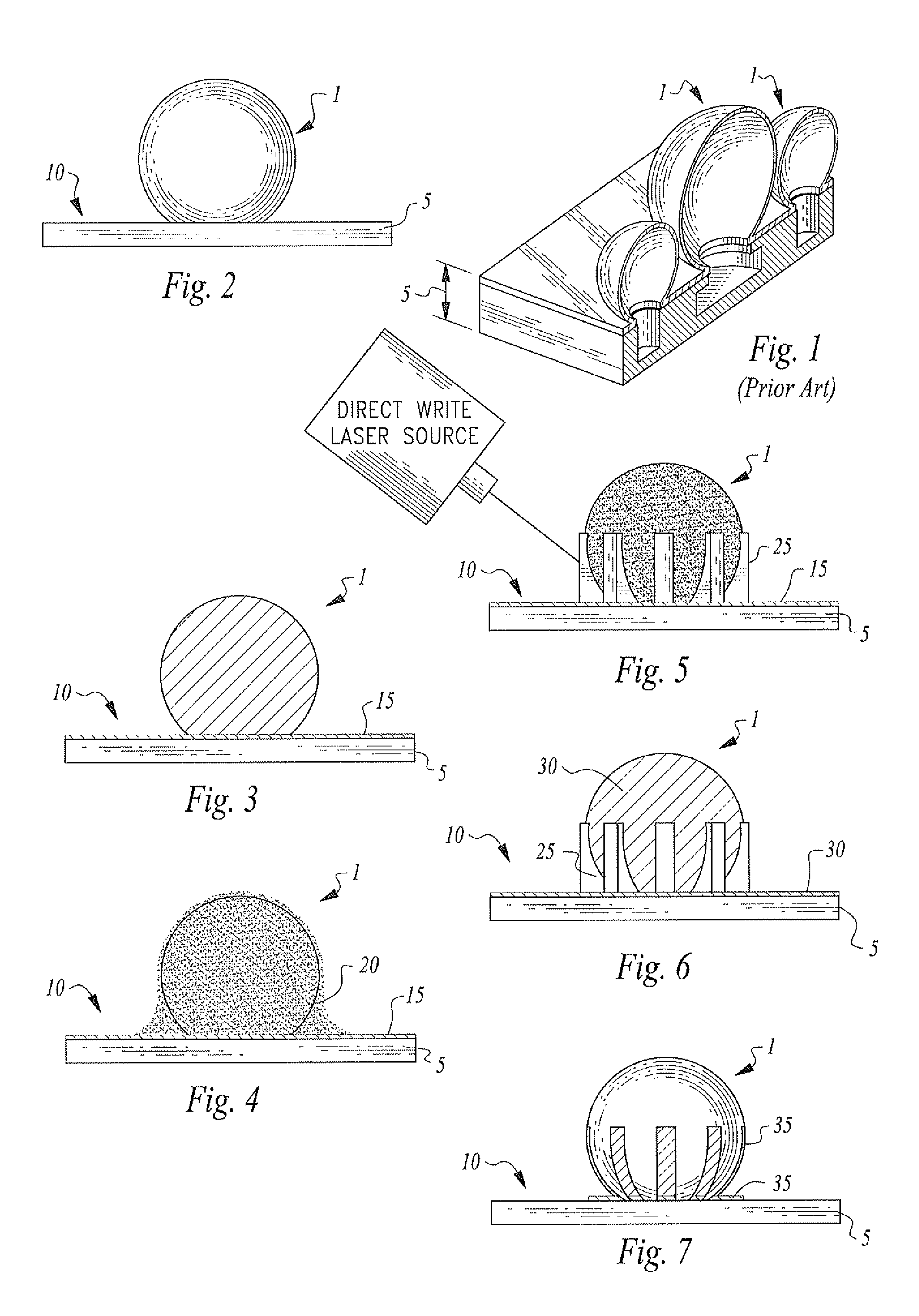
[0033]Turning now to the figures wherein like numerals define like elements among the several views, a method for defining a electrically conductive metalized structure, which may comprise an electrode or trace, on the surface of a three-dimensional element and a method for making the same is disclosed.

[0034]With respect to FIG. 1, a plurality of three-dimensional elements 1 are depicted. The illustrated three-dimensional elements 1 depict a plurality of prior art glass microspheres for use as glass shell resonator elements such as disclosed in U.S. Pat. No. 7,694,531, supra.

[0035]Three-dimensional elements 1 are disposed on substrate 5 which substrate material may comprise a silicon material or a glass material or both, such as in a Pyrex-Si wafer stack. The substrate comprises a first surface 10.

[0036]FIG. 2 illustrates a side view of an exemplar three-dimensional structure 1 in the form of a glass shell resonator structure disposed on first surface 10.

[0037]As depicted in FIG. 3,...


PUM

PropertyMeasurementUnit
diameteraaaaaaaaaa
thicknessaaaaaaaaaa
electrically conductiveaaaaaaaaaa

Abstract

A method for defining an electrically conductive metalized structure, which may comprise an electrode or trace, on the surface of a three-dimensional element. The three-dimensional element may comprise a glass microsphere or shell resonator. A laser direct write grayscale photolithographic process is used in conjunction with electrically conductive metal deposition processes to define one or more electrically conductive metal structures on the surfaces of the three dimensional element.

Description

CROSS-REFERENCE TO RELATED APPLICATIONS[0001]This application claims the benefit of U.S. Provisional Patent Application No. 61 / 455,125, filed on Oct. 13, 2010 entitled “Method for Feature Metalization of Spherical Surfaces and a Device Made from the Method” pursuant to 35 USC 119, which application is incorporated fully herein by reference.STATEMENT REGARDING FEDERALLY SPONSORED RESEARCH AND DEVELOPMENT[0002]N / ABACKGROUND OF THE INVENTION[0003]1. Field of the Invention[0004]The invention relates generally to the field of photolithographic technologies used in electronic fabrications processes.[0005]More specifically, the invention relates to a method for defining an electrically conductive metal structure on a three-dimensional element which, in one embodiment, may comprise defining an electrically conductive metallic trace, pattern, electrode or other structure on the surface of a glass microsphere or spherical shell resonator.[0006]The invention further relates to a device made fr...

Claims


Application Information

Patent Timeline
Patent Type & Authority Applications(United States)
IPC IPC(8): B32B3/00G03F7/20
CPCY10T428/24802B32B2559/00Y10T428/24926B32B15/16
Inventor YAMAGUCHI, JAMESBOYD, W. ERIC
Owner PFG IP
Why Eureka
Try Eureka