Active device array substrate, display panel and repair method

a technology of active devices and array substrates, applied in static indicating devices, non-linear optics, instruments, etc., can solve the problems of devices not being fully or partially operated, sealant cannot be completely cured, etc., and achieve the effect of reducing rc loading

Inactive Publication Date: 2012-02-02
AU OPTRONICS CORP
View PDF2 Cites 4 Cited by
  • Summary
  • Abstract
  • Description
  • Claims
  • Application Information

AI Technical Summary

Benefits of technology

[0008]The invention is directed to an active device array substrate capable of effectively reducing RC loading when signals are transmitted by a driving circuit.

Problems solved by technology

Hence, when the sealant is cured by ultraviolet light, the sealant cannot be completely cured due to the metal gate in the bottom gate TFT.
As such, devices cannot be fully or partially operated.

Method used


Image

  • Active device array substrate, display panel and repair method
  • Active device array substrate, display panel and repair method
  • Active device array substrate, display panel and repair method

Examples


Embodiment Construction

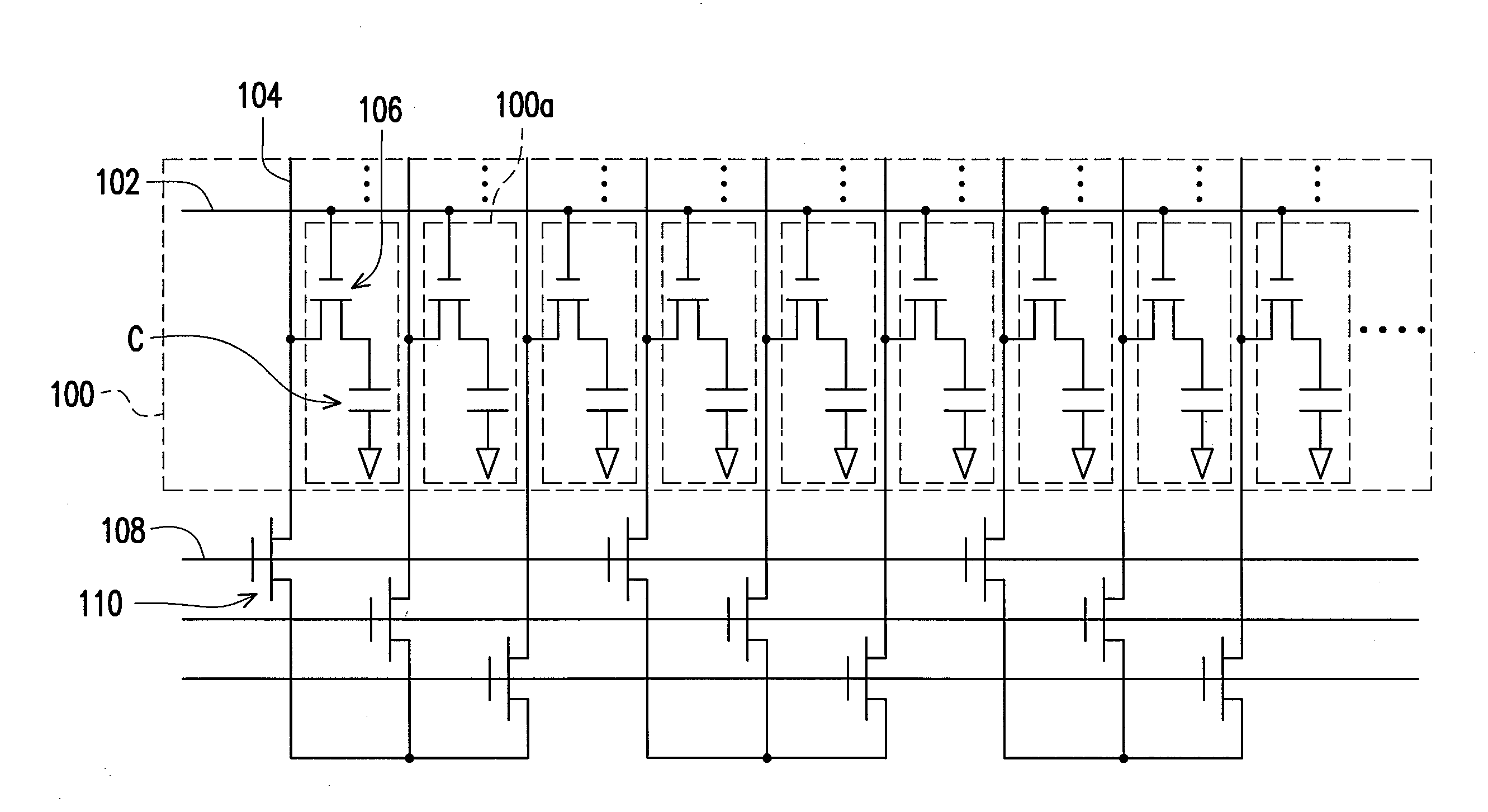
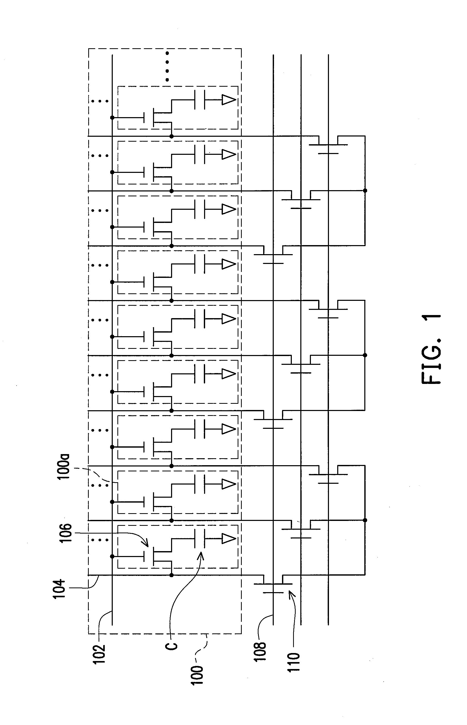
[0040]FIG. 1 is a schematic diagram illustrating circuits in an active device array substrate according to an embodiment of the invention. For illustrative and descriptive purposes, only one scan line is depicted in FIG. 1, while there are actually a plurality of scan lines in the active device array substrate. As indicated in FIG. 1, the active device array substrate has a display region 100. Besides, the active device array substrate includes a substrate, first signal lines, second signal lines, active devices 106, pixel electrodes (not shown), a bus line 108, and a switch device 110. The substrate is depicted in FIG. 2 and will be described later. In this embodiment, the first signal lines are scan lines 102, and the second signal lines are data lines 104.

[0041]The scan lines 102 and the data lines 104 are arranged on the substrate and interlaced with each other to define a plurality of pixel regions 100a in the display region 100. The active devices 106 are disposed correspondin...


PUM


Abstract

A display panel, a repair method, and an active device array substrate including a substrate, first and second signal lines, active devices, pixel electrodes, a bus line, and a switch device are provided. The bus line and the switch device are disposed outside a display region of the active device array substrate. The switch device has a gate coupled to the bus line, a first electrode coupled to a signal source, and a second electrode coupled to one of the first signal lines. The first and second electrodes are comb-shaped. The first electrode includes first fingers parallel to one another and a first connection portion connected to the first fingers. The second electrode includes second fingers parallel to one another and a second connection portion connected to the second fingers. The first and second fingers are arranged alternately. A portion of the first electrode is located outside the gate.

Description

CROSS-REFERENCE TO RELATED APPLICATION[0001]This application claims the priority benefit of Taiwan application serial no. 99125127, filed on Jul. 29, 2010. The entirety of the above-mentioned patent application is hereby incorporated by reference herein and made a part of this specification.BACKGROUND OF THE INVENTION[0002]1. Field of the Invention[0003]The invention relates to an active device array substrate, a display panel, and a repair method. More particularly, the invention relates to an active device array substrate, a display panel, and a repair method capable of reducing resistance-capacitance (RC) loading during signal transmission and preventing short circuit caused by metallic particles.[0004]2. Description of Related Art[0005]In normal displays, bottom gate thin film transistors (TFT) have high parasitic capacitance (Cgd and Cgs), and therefore significant RC loading is often generated during signal transmission if the bottom gate TFT serves as the TFT in a driving cir...

Claims


Application Information

Patent Timeline
Patent Type & Authority Applications(United States)
IPC IPC(8): G09G3/20
CPCG02F1/136259
Inventor CHIU, HAO-LINKAO, YIH-CHYUN
Owner AU OPTRONICS CORP
Why Eureka
Try Eureka