Organic el display panel and method of manufacturing the same
a technology of organic el and display panels, which is applied in the direction of basic electric elements, electrical equipment, semiconductor devices, etc., can solve the problems of possible complex manufacturing of organic el display panels and increase production costs, and achieve the effect of preventing anomalous light emission
- Summary
- Abstract
- Description
- Claims
- Application Information
AI Technical Summary
Benefits of technology
Problems solved by technology
Method used
Image
Examples
embodiments of invention
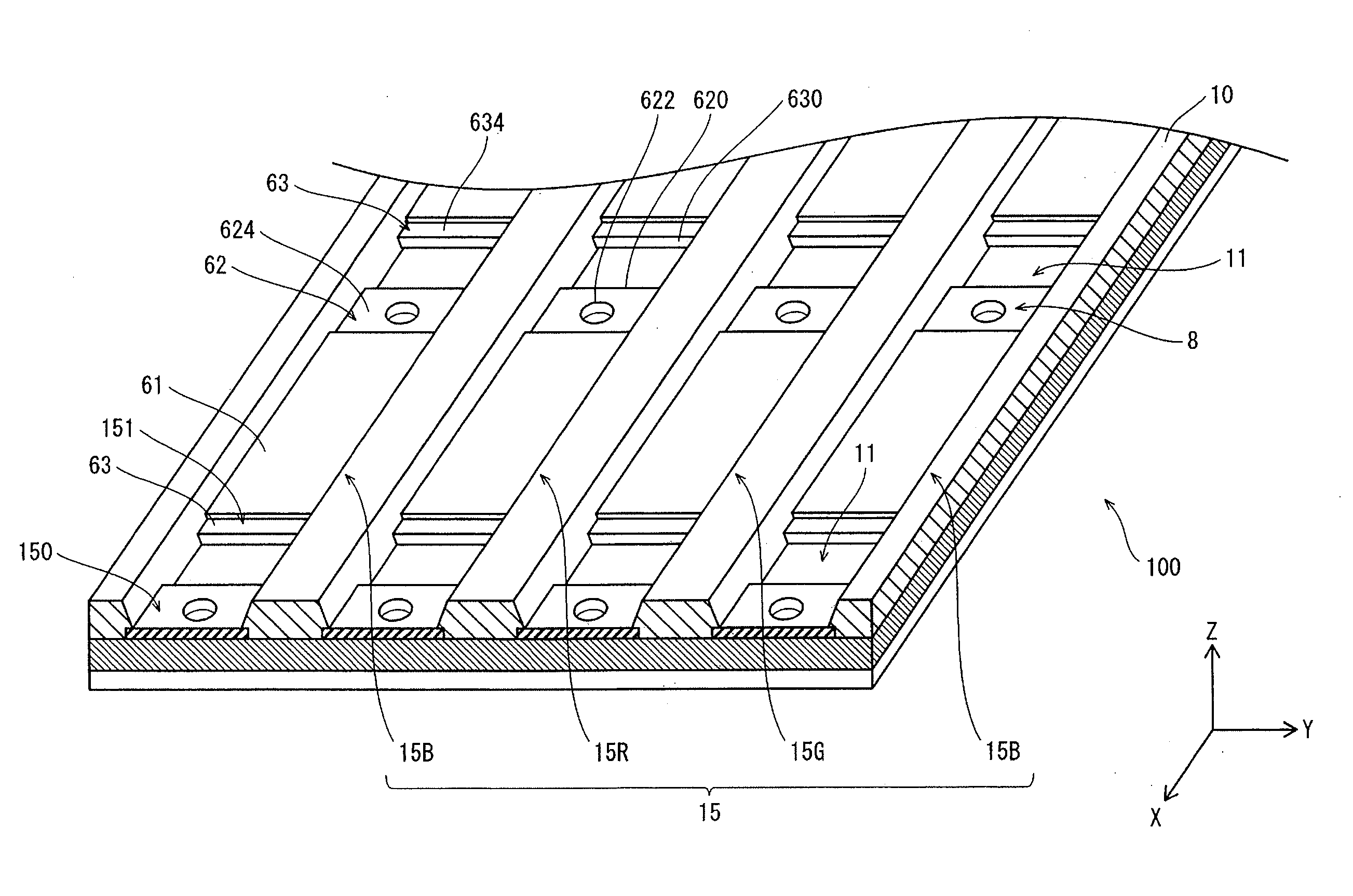
[0031]In order to solve the above-stated problems, one aspect of the present invention is an organic EL display panel comprising: a substrate; a thin-film transistor layer formed on the substrate; an interlayer insulating film formed above the thin-film transistor layer; a plurality of strip-shaped barrier ribs that are arranged in parallel on the interlayer insulating film; a plurality of first electrode groups, each of which consists of first electrodes that are arranged in a line and is arranged between two adjacent ones of the barrier ribs, each of the first electrodes including a transparent conductive film and a reflective metal film that is formed of a metal material; a plurality of light-emitting layers each formed to cover a different one of the first electrode groups; and a second electrode formed above the light-emitting layers, wherein each of the first electrodes is formed such that: at least one of end portions of the first electrode in a parallel direction with respec...
first embodiment
Structure of Organic EL Display Panel 100
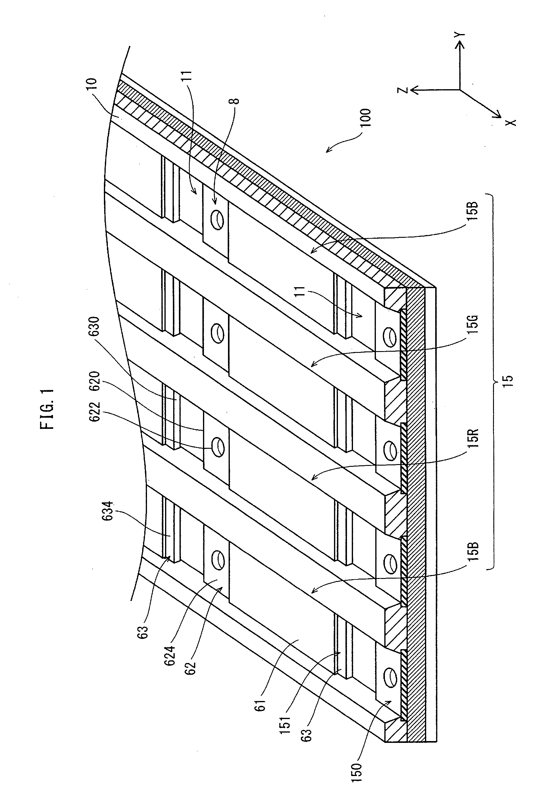
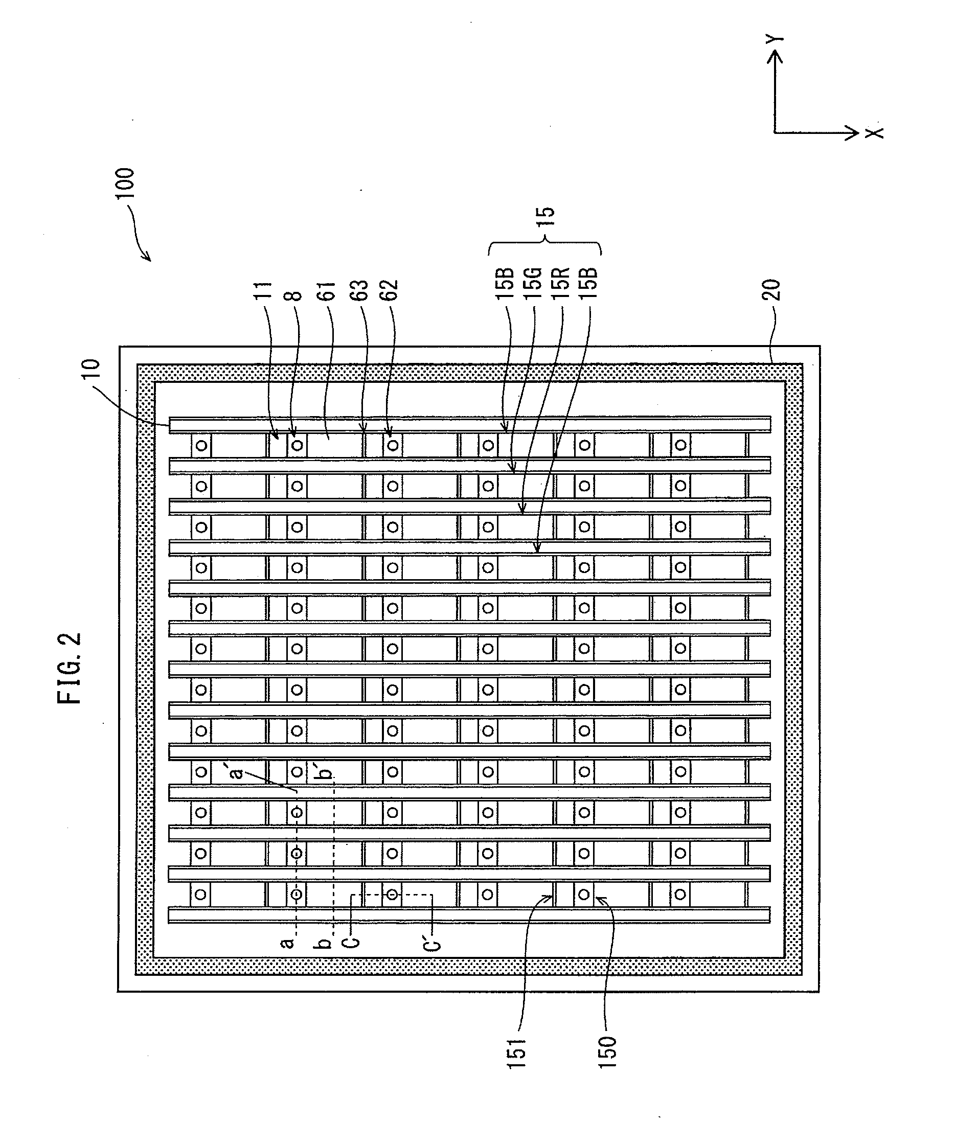
[0056]FIG. 1 is a perspective view partially showing a structure of a top-emission organic EL display panel 100 (hereinafter, simply referred to as a “panel 100”) of a first embodiment of the present invention. FIG. 2 shows a front view of the panel 100. Note that an upper electrode and a sealing layer, for example, that are provided above a light-emitting layer 7 are omitted for describing a lower electrode 6, in FIG. 1 and FIG. 2. FIG. 3 is a partial cross-section view (cross section view of c-c′ of FIG. 2) that schematically shows the structure of the panel 100.
[0057]In the panel 100, organic EL elements 15 (15R, 15B and 15G) each having a light-emitting layer 7 of one of R, G and B colors are disposed in a row direction (a Y direction) as sub pixels. A set of three adjacent sub pixels functions as one pixel.
[0058]In the panel 100 as a whole, organic EL elements 15R, 15G and 15B are disposed in a matrix in both the column and row direction...
second embodiment
[0091]The following describes a second embodiment of the present invention, focusing on differences from the first embodiment.
[0092]The panel 100 of the first embodiment has a structure in which the reflective metal film 60 is formed directly on the planarizing film 4. However, the structure of the panel is not limited to this. A separate conductive film may be formed between the planarizing film 4 and the reflective metal film 60.
[0093]Specifically, a contact layer 65 may be formed between the planarizing film 4 and the reflective metal film 60 as shown in the cross-section view of a panel 100A of FIG. 4. The contact layer 65 is formed using a metal such as Ti or Cr, or a conductive metal oxide such as ITO or IZO. In this way, the reflective metal film 60 can be adhered tightly to an upper surface of the planarizing film 4 effectively.
[0094]The panel 100A having such a structure can achieve effects of preventing the short between the single-film portion 150 (151) of lower electrode...
PUM
 Abstract
Description
Claims
Application Information
 - R&D
- Intellectual Property
- Life Sciences
- Materials
- Tech Scout
- Unparalleled Data Quality
- Higher Quality Content
- 60% Fewer Hallucinations
Browse by: Latest US Patents, China's latest patents, Technical Efficacy Thesaurus, Application Domain, Technology Topic, Popular Technical Reports.
© 2025 PatSnap. All rights reserved.Legal|Privacy policy|Modern Slavery Act Transparency Statement|Sitemap|About US| Contact US: help@patsnap.com


