Organic EL display panel and method of manufacturing the same
a technology of organic el and display panels, which is applied in the direction of discharge tubes/lamp details, thermoelectric devices, discharge tubes/lamp details, etc., can solve the problems of possible complex manufacture of organic el display panels and increase production costs, and achieve the effect of preventing anomalous light emission
- Summary
- Abstract
- Description
- Claims
- Application Information
AI Technical Summary
Benefits of technology
Problems solved by technology
Method used
Image
Examples
first embodiment
[0058][First Embodiment]
[0059](Structure of Organic EL Display Panel 100)
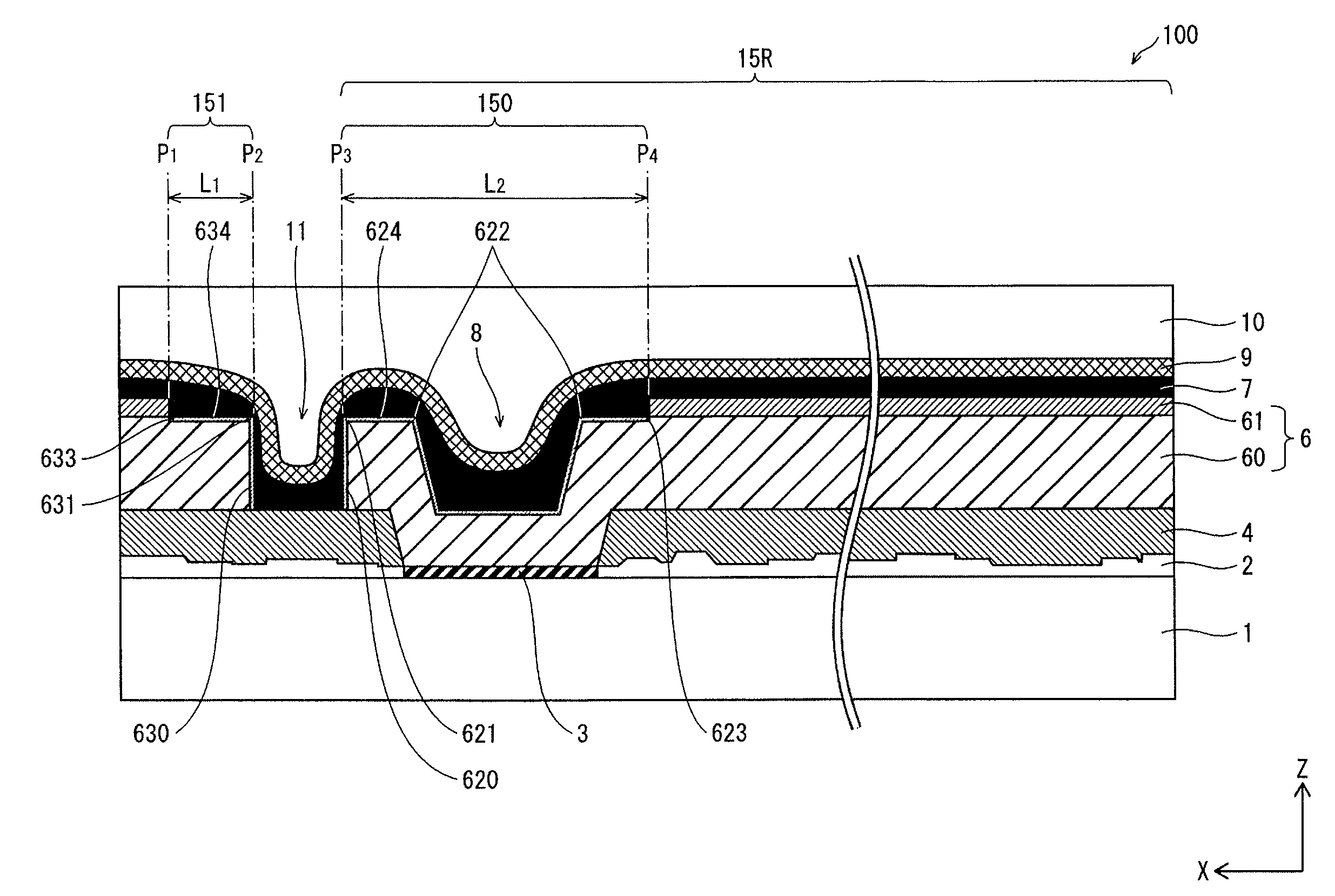
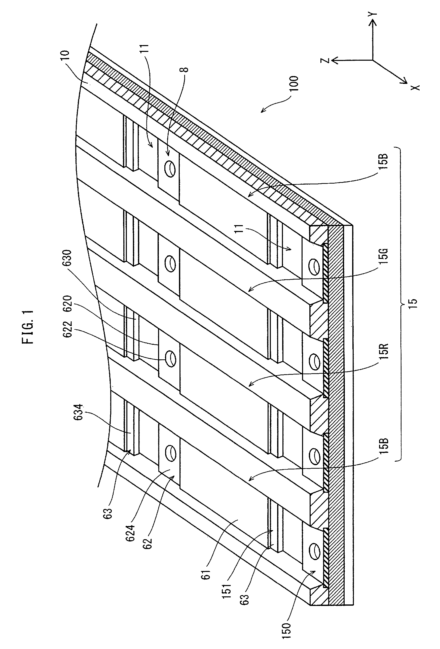
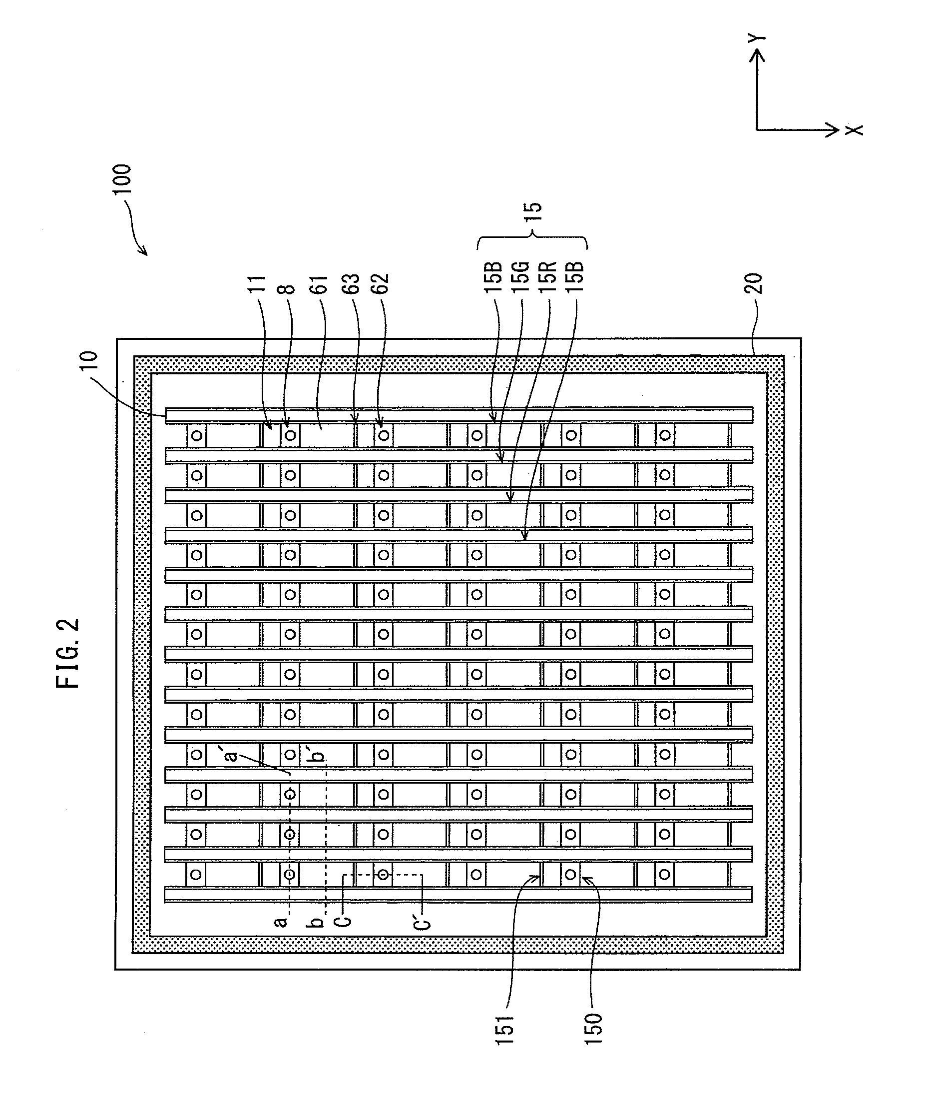
[0060]FIG. 1 is a perspective view partially showing a structure of a top-emission organic EL display panel 100 (hereinafter, simply referred to as a “panel 100”) of a first embodiment of the present invention. FIG. 2 shows a front view of the panel 100. Note that an upper electrode and a sealing layer, for example, that are provided above a light-emitting layer 7 are omitted for describing a lower electrode 6, in FIG. 1 and FIG. 2. FIG. 3 is a partial cross-section view (cross section view of c-c′ of FIG. 2) that schematically shows the structure of the panel 100.
[0061]In the panel 100, organic EL elements 15 (15R, 15B and 15G) each having a light-emitting layer 7 of one of R, G and B colors are disposed in a row direction (a Y direction) as sub pixels. A set of three adjacent sub pixels functions as one pixel.
[0062]In the panel 100 as a whole, organic EL elements 15R, 15G and 15B are disposed in a matrix in b...
second embodiment
[0095][Second Embodiment]
[0096]The following describes a second embodiment of the present invention, focusing on differences from the first embodiment.
[0097]The panel 100 of the first embodiment has a structure in which the reflective metal film 60 is formed directly on the planarizing film 4. However, the structure of the panel is not limited to this. A separate conductive film may be formed between the planarizing film 4 and the reflective metal film 60.
[0098]Specifically, a contact layer 65 may be formed between the planarizing film 4 and the reflective metal film 60 as shown in the cross-section view of a panel 100A of FIG. 4. The contact layer 65 is formed using a metal such as Ti or Cr, or a conductive metal oxide such as ITO or IZO. In this way, the reflective metal film 60 can be adhered tightly to an upper surface of the planarizing film 4 effectively.
[0099]The panel 100A having such a structure can achieve effects of preventing the short between the single-film portion 150...
PUM
 Abstract
Description
Claims
Application Information
 - R&D
- Intellectual Property
- Life Sciences
- Materials
- Tech Scout
- Unparalleled Data Quality
- Higher Quality Content
- 60% Fewer Hallucinations
Browse by: Latest US Patents, China's latest patents, Technical Efficacy Thesaurus, Application Domain, Technology Topic, Popular Technical Reports.
© 2025 PatSnap. All rights reserved.Legal|Privacy policy|Modern Slavery Act Transparency Statement|Sitemap|About US| Contact US: help@patsnap.com


