Display device

a display module and display technology, applied in the field of display devices, can solve the problems of increasing the number of flexible printed circuits and the larger size of circuitry, and achieve the effects of increasing the number of pixels in the display module, reducing the number of electrical lines connected to the active matrix substrate, and simple structur

Inactive Publication Date: 2012-01-19
SHARP KK
View PDF11 Cites 8 Cited by
  • Summary
  • Abstract
  • Description
  • Claims
  • Application Information

AI Technical Summary

Benefits of technology

[0006]In such liquid crystal display devices, liquid crystal panels (display modules) with larger screen size and higher definition require increased numbers of pixels.
[0008]An object of the present invention is to provide a display device with a simple structure where the number of electrical lines connected to the active matrix substrate can be reduced even when the number of pixels in the display module is increased.
[0010]According to the present embodiment, it is possible to provide a display device with a simple structure where the number of electrical lines connected to the active matrix substrate can be reduced even when the number of pixels in the display module is increased.

Problems solved by technology

However, in such a conventional liquid crystal display device, an increased number of pixels of a liquid crystal panel leads to an increased number of electrical lines connected to the active matrix substrate.
This causes problems such as an increased number of flexible printed circuits, larger size of circuitry or the like.

Method used


Image

  • Display device
  • Display device
  • Display device

Examples


embodiments

[0026]Preferred embodiments of display devices will now be described with reference to the drawings. In the description below, transmissive liquid crystal display devices are set forth as examples. It should be noted that the sizes of the components in the drawings do not exactly represent the sizes of the actual components nor the size ratios of the components.

first embodiment

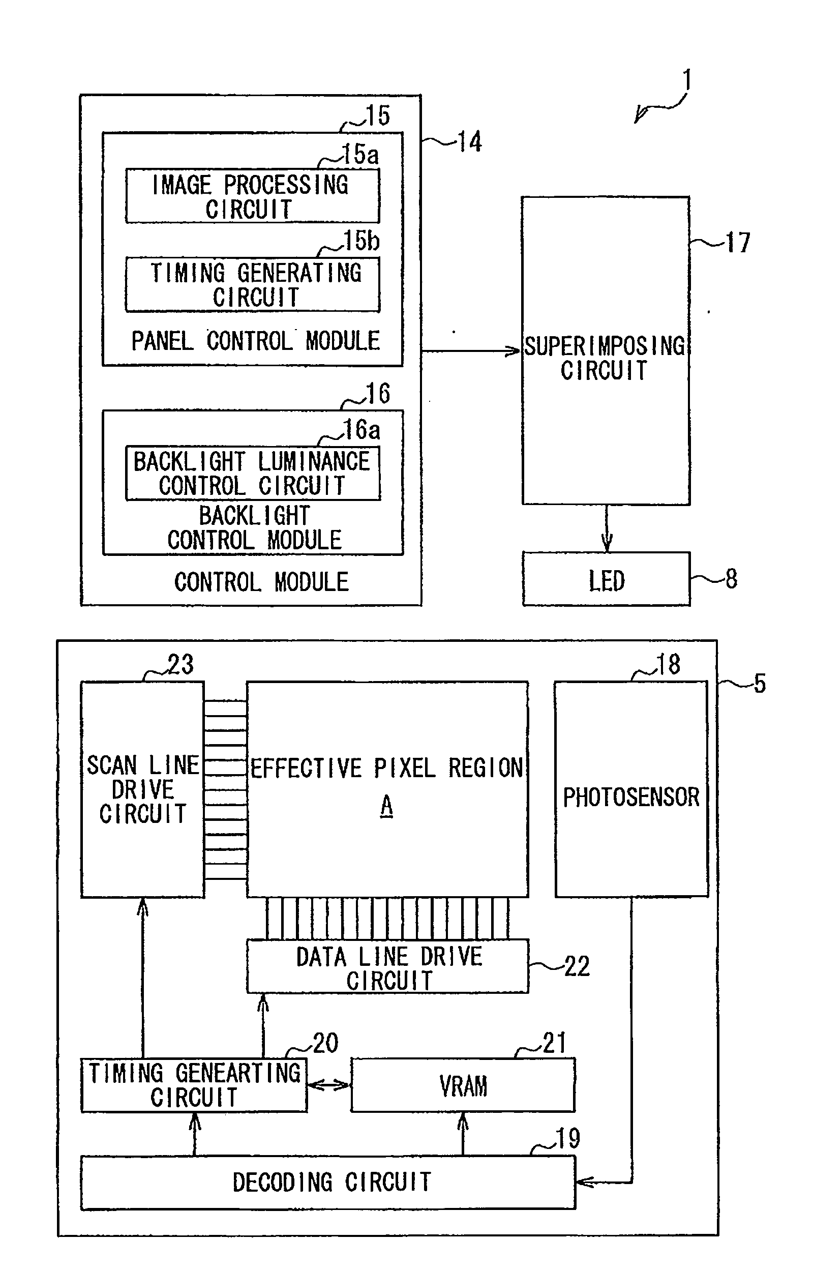
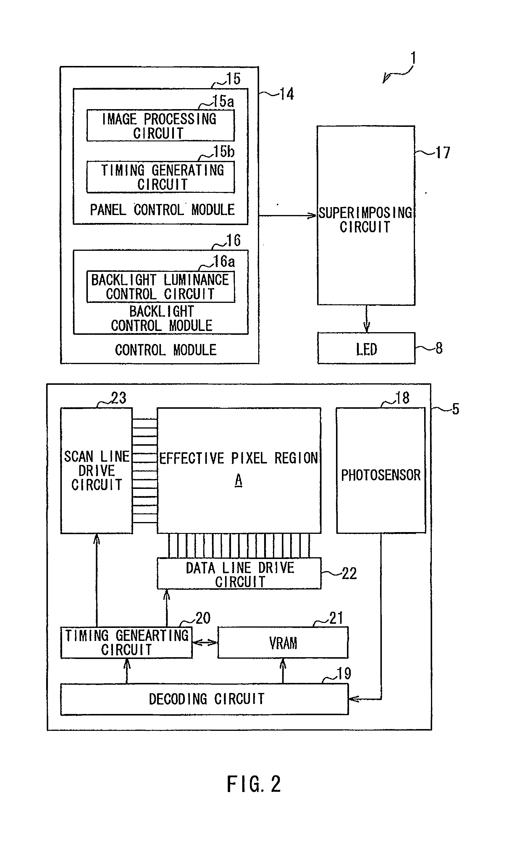
[0027]FIG. 1 illustrates a liquid crystal display device according to a first embodiment of the present invention. In FIG. 1, a liquid crystal display device 1 of the present embodiment includes a liquid crystal panel 2 as a display module, where the upper side in FIG. 1 is the viewer's side (display side), and a backlight device 3 as a backlight module that is located on the non-display side (lower side in FIG. 1) of the liquid crystal panel 2 and generates illumination light that illuminates the liquid crystal panel 2.

[0028]The liquid crystal panel 2 includes a pair of substrates, i.e. a CF (color filter) substrate 4 and an active matrix substrate 5, and polarizers 6 and 7 that sandwich the CF substrate 4 and the active matrix substrate 5. A liquid crystal layer, not shown, is sandwiched between the CF substrate 4 and the active matrix substrate 5. The CF substrate 4 and the active matrix substrate 5 each may be a plate of a transparent glass material or a transparent synthetic re...

second embodiment

[0063]FIG. 6 illustrates the configuration of main portions of a liquid crystal display device according to a second embodiment of the present invention. In the drawing, the present embodiment is different from the first embodiment mainly in that a solar cell unit, instead of a photosensor unit, is provided on the active matrix substrate. Note that the components common to the first and second embodiments are labeled with the same numerals, and the overlapping description is omitted.

[0064]Specifically, as shown in FIG. 6, in a liquid crystal display device 1 of the present embodiment, a solar cell unit 27 as a light-electricity transducer is mounted on the active matrix substrate 5 outside the effective pixel region A. The solar cell unit 27 is provided on the active matrix substrate 5 in such a way that its light receiving side is opposite the light guide plate 9 (FIG. 1). In other words, the solar cell unit 27 is configured to detect only light from the light-emitting diode 8, and...


PUM


Abstract

A display device with a simple structure is provided where the number of electrical lines connected to the active matrix substrate can be reduced even when the number of pixels in the display module is increased. A liquid crystal display device includes a superimposing circuit (superimposing module) that superimposes a lighting signal for a light-emitting diode (light source) on a drive signal for a data line drive circuit (drive circuit) and a scan line drive circuit (drive circuit) to generate a superimposed signal. On the active matrix substrate are provided a photosensor unit (light-electricity transducer) that receives light from the light-emitting diode and outputs an electrical signal corresponding to the received light, and a decoding circuit (decoding module) that decodes the electrical signal from the photosensor unit to the drive signal for the data line drive circuit and the scan line drive circuit.

Description

TECHNICAL FIELD[0001]The present invention relates to display devices, more particularly to non-emissive displays such as liquid crystal display devices.BACKGROUND ART[0002]Liquid crystal display devices, for example, are widely used in liquid crystal television sets, monitors, cell phones or the like, in the form of flat panel displays, which are thinner and lighter than conventional cathode-ray tubes. Such a liquid crystal display device includes a backlight that emits light and a liquid crystal panel that serves as a shutter for light from the backlight to display a desired image.[0003]Further, in such a liquid crystal display device, an arrangement in which a plurality of data lines (source lines) and a plurality of scan lines (gate lines) are laid out in a matrix is known. In such a liquid crystal display device, an active matrix substrate is used for a liquid crystal panel as a display module displaying information, where the active matrix substrate includes pixels each having...

Claims


Application Information

Patent Timeline
IPC IPC(8): G09G5/10
CPCG09G3/3406G09G3/3648G09G2360/141G09G2320/0646G09G2320/062
Inventor MIZUBUCHI, NAOKI
Owner SHARP KK
Why Eureka
Try Eureka