Method of programming a semiconductor memory device
a memory device and semiconductor technology, applied in the field of semiconductor memory device programming, can solve problems such as inadvertent variations of threshold voltages, and achieve the effect of lessening interferen
- Summary
- Abstract
- Description
- Claims
- Application Information
AI Technical Summary
Benefits of technology
Problems solved by technology
Method used
Image

Examples
first embodiment
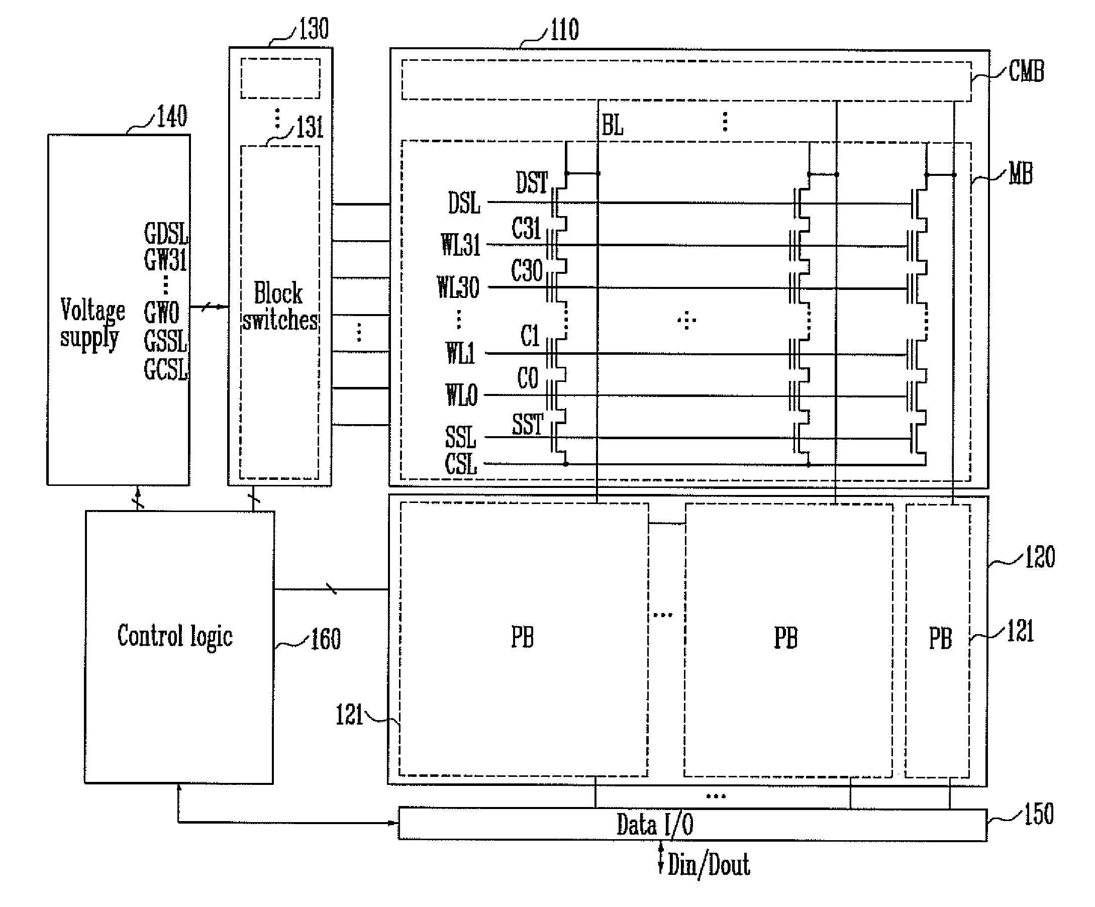
[0092]FIG. 5 shows waveforms of the program and verifying voltages in a programming operation according to the present invention, which is described with reference to the page buffer 121 of FIG. 2 and the threshold voltage distribution diagram of FIG. 3.
[0093]The program and verifying voltages shown in FIG. 5 are to be applied to a selected word line (Sel WL) during an MSB page programming, for which the program voltage is applied twice at one time. That is, the selected word line are sequentially applied with a first program start voltage Vs1 for shifting the memory cells into the threshold voltage distributions B and C, and a second program start voltage Vs2 for shifting the memory cells into the threshold voltage distribution D.
[0094]Hereinafter, memory cells to be programmed in the threshold voltage distribution B are referred to as ‘first memory cell group’; memory cells to be programmed in the threshold voltage distribution C are referred to as ‘second memory cell group’; memo...
second embodiment
[0174]In a second embodiment, program voltages are sequentially applied to program first to third memory cell groups, as described with reference to a page buffer including a dynamic latch.
[0175]FIGS. 7A through 7D illustrate page buffers according to the second embodiment of the present invention.
[0176]The entire configuration of the page buffer is briefly shown in FIG. 7A. Latch circuits of the page buffer of FIG. 7A are detailed in FIGS. 7B to 7D, respectively. FIGS. 7A to 7D depict the parts of the semiconductor memory device modified for the second embodiment, where other parts of which may be same as those of the first embodiment.
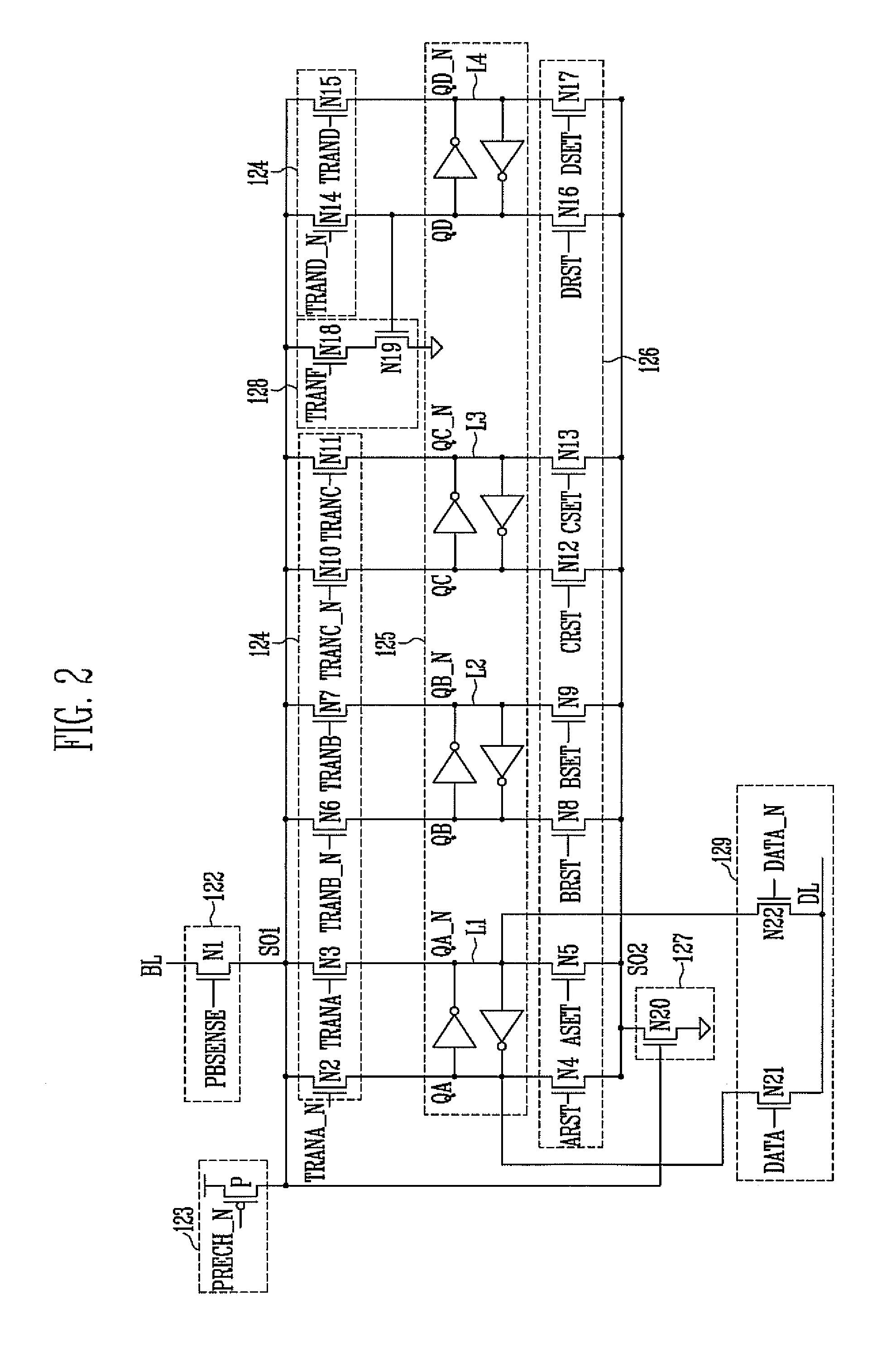
[0177]Referring to FIG. 7A, a page buffer 121 including a dynamic latch is comprised of a bit-line connection circuit 710, a precharging circuit 720, and first to fourth latch circuits 730, 740, 750 and 760.
[0178]The bit-line connection circuit 710 is provided to electrically connect a bit line BL with a first sensing node S01. The bit-line connection...
PUM
 Abstract
Description
Claims
Application Information
 - R&D
- Intellectual Property
- Life Sciences
- Materials
- Tech Scout
- Unparalleled Data Quality
- Higher Quality Content
- 60% Fewer Hallucinations
Browse by: Latest US Patents, China's latest patents, Technical Efficacy Thesaurus, Application Domain, Technology Topic, Popular Technical Reports.
© 2025 PatSnap. All rights reserved.Legal|Privacy policy|Modern Slavery Act Transparency Statement|Sitemap|About US| Contact US: help@patsnap.com