
Method of programming nonvolatile memory device

Inactive Publication Date: 2011-12-01
SK HYNIX INC
View PDF0 Cites 13 Cited by
  • Summary
  • Abstract
  • Description
  • Claims
  • Application Information

AI Technical Summary

Benefits of technology

[0067]In accordance with the present disclosure, the difference between the threshold voltages of selected memory cells and their neighboring memory cells is reduced when the selected memory cells are programmed. Accordingly, interference between neighboring memory cells resulting from a difference in the threshold voltage can be reduced, and so reliability of a program operation can be improved.

Problems solved by technology

As the difference between the threshold voltages of cells existing near the selected memory cell increases, more interference may be generated because of a potential.
The interference is further increased because the gap between the cells is narrowed with an increase in the degree of integration of memory devices.
In particular, reliability is gradually being deteriorated because of greater interference resulting from the recent high degree of integration of memory devices.

Method used


Image

  • Method of programming nonvolatile memory device
  • Method of programming nonvolatile memory device
  • Method of programming nonvolatile memory device

Examples


Embodiment Construction

[0031]Hereinafter, some exemplary embodiments of the present disclosure will be described in detail with reference to the accompanying drawings. The figures are provided to allow those having ordinary skill in the art to understand the scope of the exemplary embodiments of the disclosure.

[0032]Herein, “n” and “N” are indexes used to reference different elements with similar features. In this capacity, “n” and “N” may be any natural number (e.g., 0, 1, 2, 3, etc.).

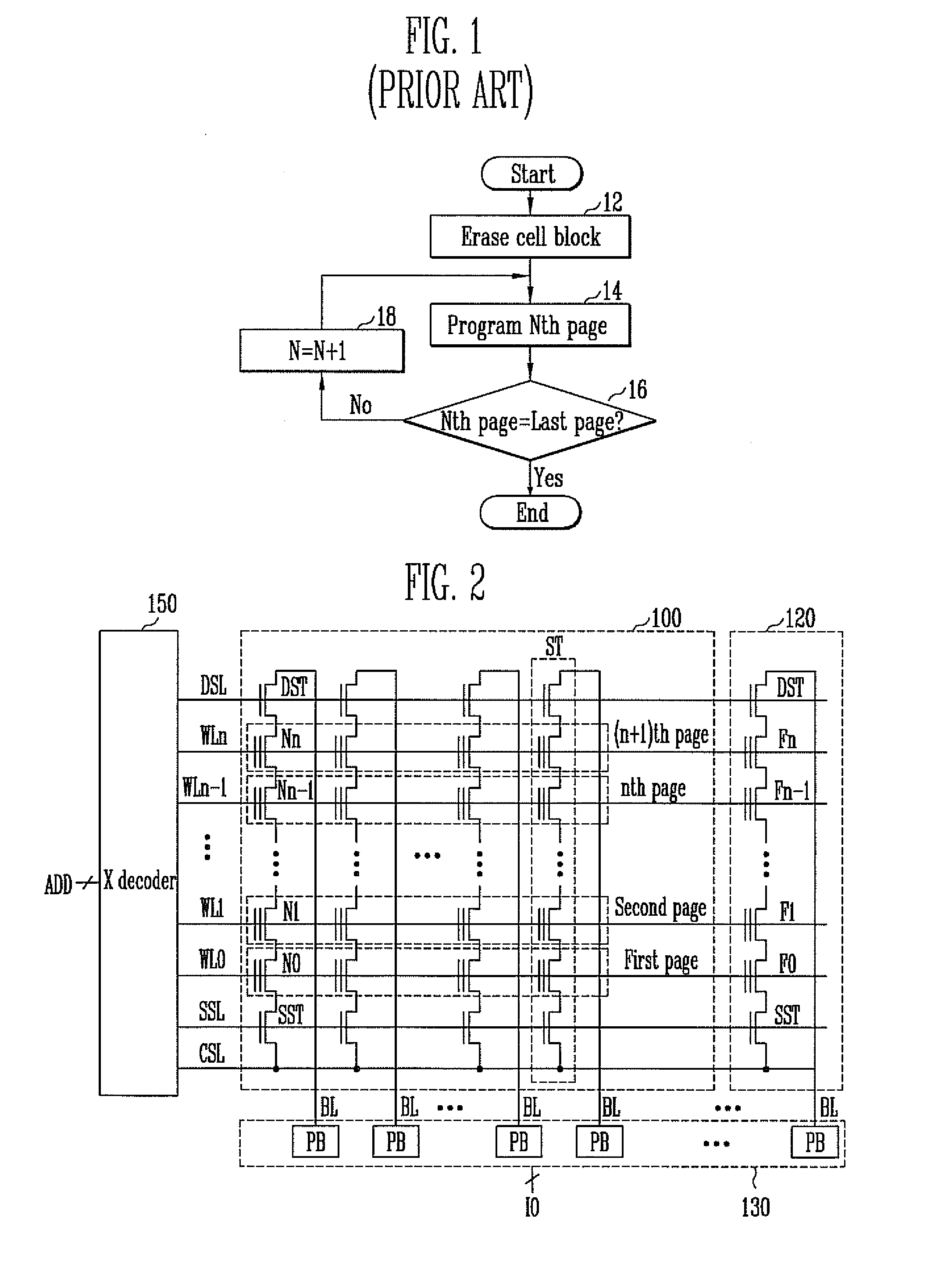
[0033]FIG. 2 is a circuit diagram showing a memory cell array of a nonvolatile memory device according to an exemplary embodiment of this disclosure.

[0034]The nonvolatile memory device includes a memory cell array 100, a flag cell array 120, a page buffer unit 130, and an X decoder 150.

[0035]The memory cell array 100 includes a plurality of strings ST. Each of the strings ST includes a drain select transistor DST, a plurality of memory cells N0 to Nn, and a source select transistor SST which are coupled in series. The gates...


PUM


Abstract

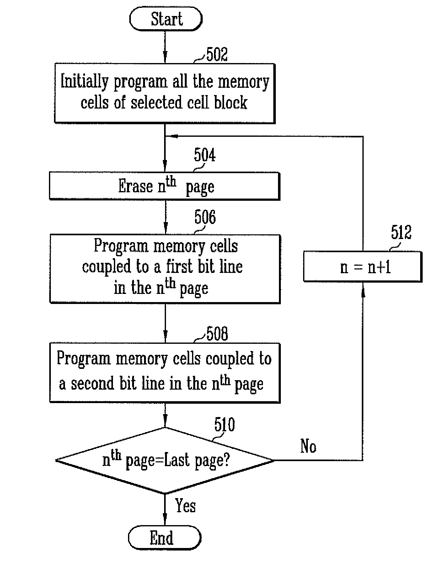
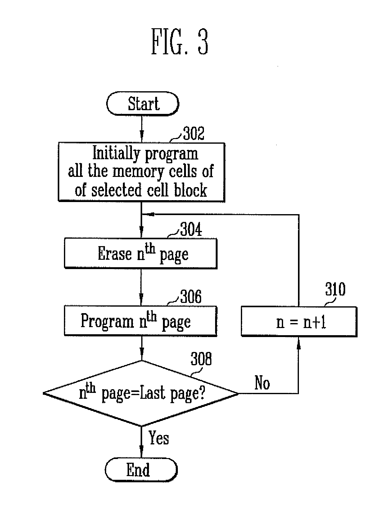
A method of programming a semiconductor device includes performing an initial program operation on all memory cells included in a selected memory cell block to set threshold voltages of all the memory cells to a voltage equal to or greater than 0 Volts, erasing memory cells of a selected page in the selected memory cell block, and programming the memory cells of the selected page.

Description

CROSS-REFERENCE TO RELATED APPLICATION[0001]Priority to Korean patent application number 10-2010-0049548 filed on May 27, 2010, the entire disclosure of which is incorporated by reference herein, is claimed.BACKGROUND[0002]Exemplary embodiments relate to a method of programming a nonvolatile memory device and, more particularly, to a method of programming a nonvolatile memory device, which is capable of reducing interference between memory cells when a program operation is performed.[0003]A nonvolatile memory device is equipped with a memory cell array for storing data. The memory cell array includes a plurality of memory cell blocks. Each of the memory cell blocks includes a plurality of memory cells coupled to a plurality of word lines. A group of the memory cells coupled to the same word line is called a page. The memory cell array includes a plurality of pages.[0004]The program operation of a nonvolatile memory device is described below.[0005]FIG. 1 is a flowchart illustrating a...

Claims


Application Information

Patent Timeline
IPC IPC(8): G11C16/10
CPCG11C11/5628G11C11/5635G11C16/107G11C16/10G11C16/0483
Inventor KIM, YONG WOOK
Owner SK HYNIX INC
Learn More