
Photo detecting pixels and x-ray detector including the same

a technology of x-ray detector and pixel, which is applied in the field of photo detecting pixels and x-ray detector, can solve the problems of inaccurate detection of x-ray image of a subject, inability to accurately perform correlation double sampling (cds), etc., and achieve the effect of reducing ktc switching nois

Active Publication Date: 2011-11-17
SAMSUNG DISPLAY CO LTD
View PDF3 Cites 7 Cited by
  • Summary
  • Abstract
  • Description
  • Claims
  • Application Information

AI Technical Summary

Benefits of technology

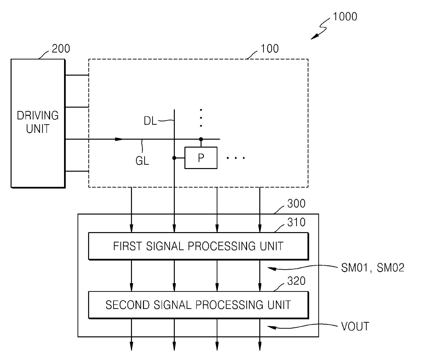
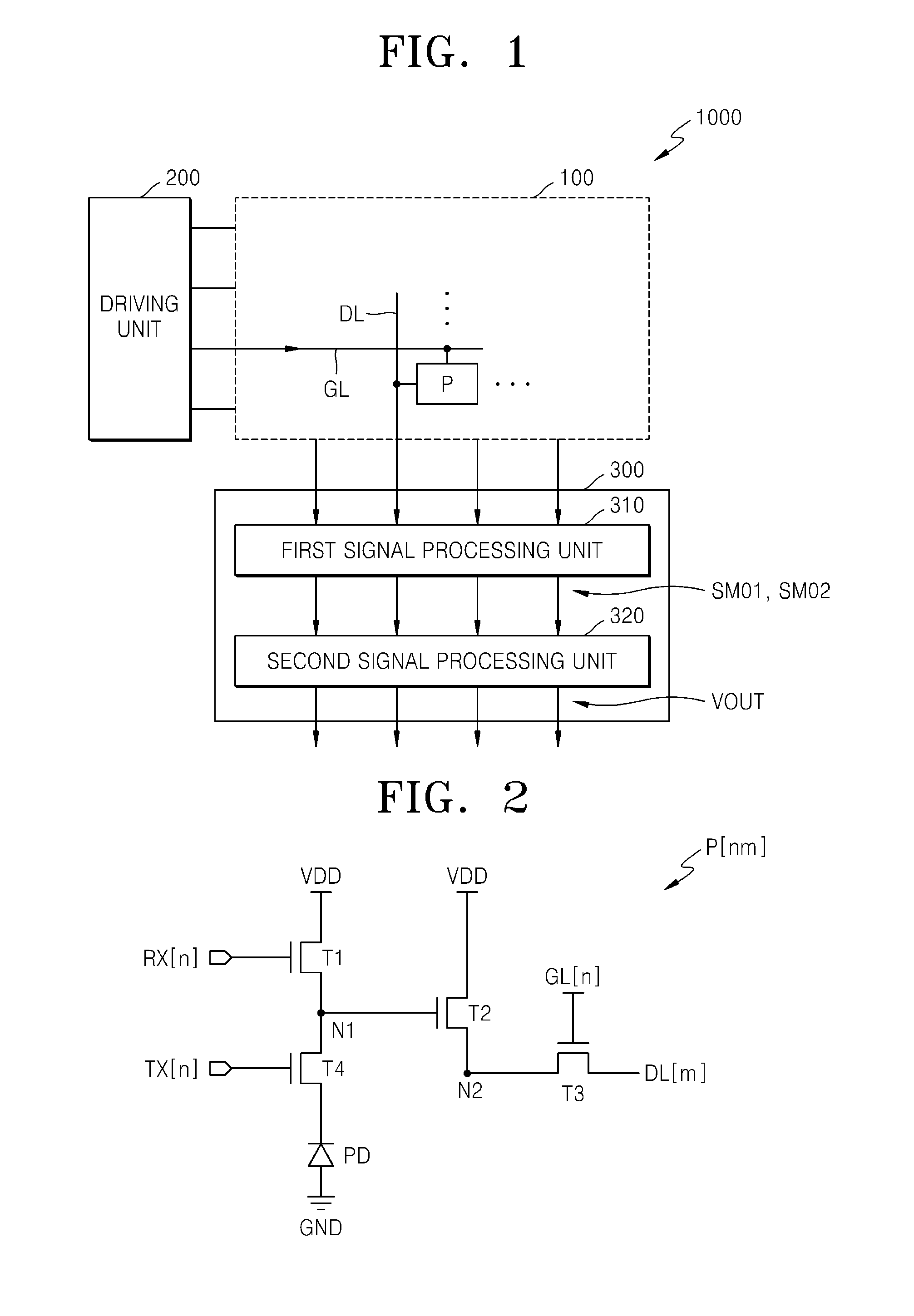
[0007]An aspect of the present invention provides photo detecting pixels capable of reducing kTC switching noise (k: Boltzmann's constant; T: temperature; C: capacitance) by accurately performing correlated double sampling (CDS), and an X-ray detector including the same.

Problems solved by technology

However, since conventional photo detecting pixels require a waiting time to receive a signal or to obtain an offset voltage, a leakage current may be generated from a pixel, and thus, correlated double sampling (CDS) may not be accurately performed.
Accordingly, an X-ray image of a subject may not be accurately detected.

Method used


Image

  • Photo detecting pixels and x-ray detector including the same
  • Photo detecting pixels and x-ray detector including the same
  • Photo detecting pixels and x-ray detector including the same

Examples


Embodiment Construction

[0031]Reference will now be made in detail to the present embodiments of the present invention, examples of which are illustrated in the accompanying drawings, wherein like reference numerals refer to the like elements throughout. The embodiments are described below in order to explain the present invention by referring to the figures.

[0032]It will be understood that, although the terms first, second, etc. may be used herein to describe various elements, these elements should not be limited by these terms. These terms are only used to distinguish one element from another.

[0033]The terminology used herein is for the purpose of describing particular embodiments only and is not intended to be limiting of exemplary embodiments of the invention. As used herein, the singular forms “a”, “an” and “the” are intended to include the plural forms as well, unless the context clearly indicates otherwise. It will be further understood that the terms “comprises”, “comprising,”, “includes” and / or “i...


PUM


Abstract

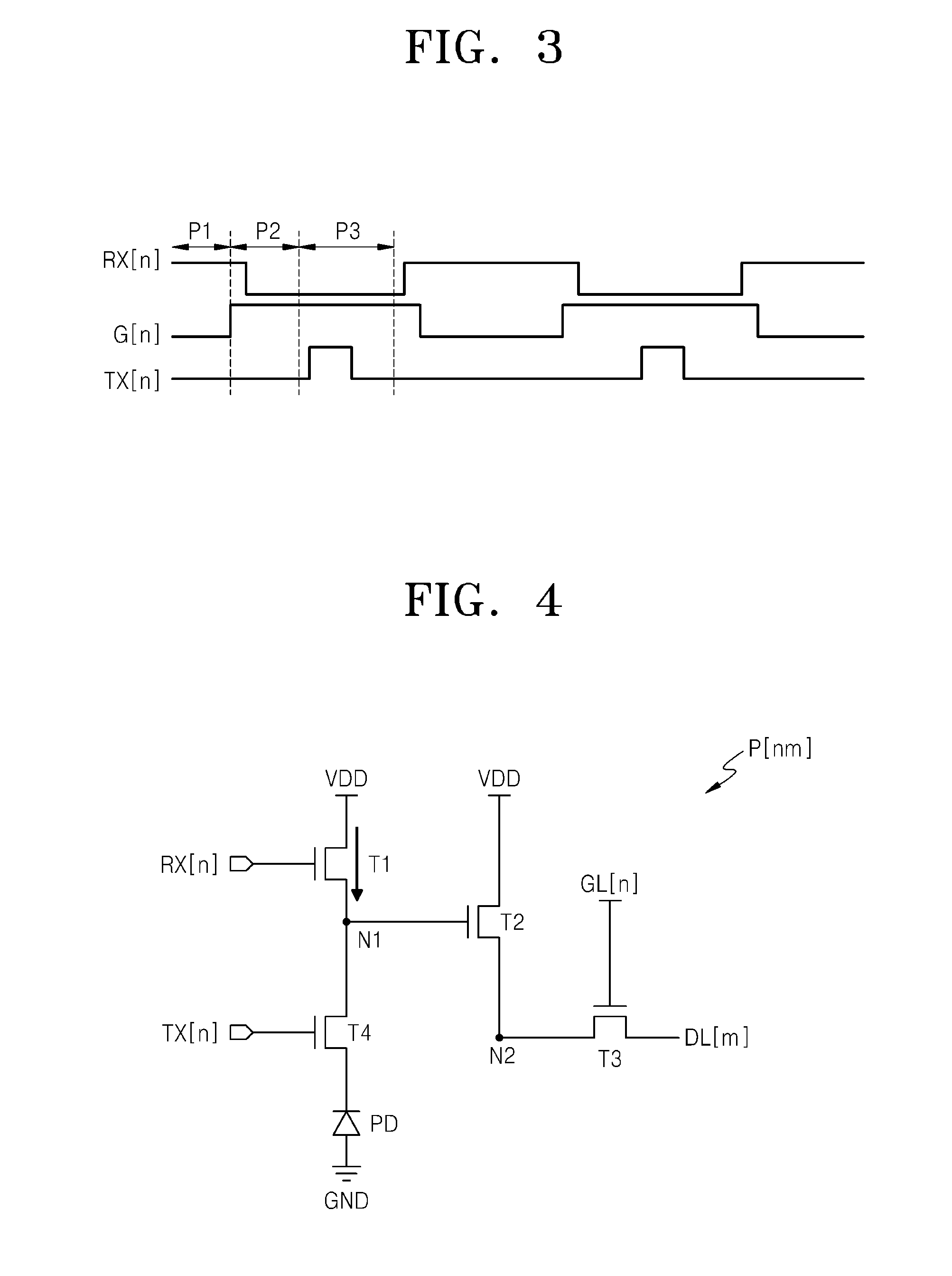
An X-ray detector including photo detecting pixels capable of reducing kTC switching noise (k: Boltzmann's constant; T: temperature; C: capacitance) by accurately performing correlated double sampling (CDS). Each of the pixels includes a first transistor comprising a first electrode connected to a first power line, a second electrode connected to a first node, and a gate electrode receiving the reset signal; a second transistor comprising a first electrode connected to the first power line, a second electrode connected to a second node, and a gate electrode connected to the first node; a third transistor comprising a first electrode connected to the second node, a second electrode connected to a data line, and a gate electrode connected to a gate line; a fourth transistor comprising a first electrode connected to the first node, a second electrode connected to a photo detecting diode, and a gate electrode receiving the control signal; and the photo detecting diode comprising a first electrode connected to the fourth transistor, and a second electrode connected to ground.

Description

CROSS-REFERENCE TO RELATED APPLICATION[0001]This application claims the benefit of Korean Patent Application No. 10-2010-0045478, filed on May 14, 2010, in the Korean Intellectual Property Office, the disclosure of which is incorporated herein by reference.BACKGROUND[0002]1. Field[0003]An aspect of the present invention relates to photo detecting pixels and an X-ray detector including the same.[0004]2. Description of the Related Art[0005]In general, an X-ray detector is used in medical diagnosis to detect and provide an X-ray image of a subject, the X-ray image being formed by an X-ray radiated from an X-ray generator, to a display apparatus. Currently, a flat panel X-ray detector employing digital radiography, that is, not requiring a photographic film, is popularly used. The flat panel X-ray detector includes a plurality of photo detecting pixels provided in a flat panel to detect an X-ray.[0006]However, since conventional photo detecting pixels require a waiting time to receive a...

Claims


Application Information

Patent Timeline
Patent Type & Authority Applications(United States)
IPC IPC(8): G01T1/24
CPCG01T1/247H04N5/363H04N5/3575H04N5/32H04N25/616H04N25/65H04N25/30
Inventor JUNG, KWAN-WOOK
Owner SAMSUNG DISPLAY CO LTD
Learn More