
Electronic component and method for making the same

Active Publication Date: 2011-11-03
MURATA MFG CO LTD
View PDF2 Cites 5 Cited by
  • Summary
  • Abstract
  • Description
  • Claims
  • Application Information

AI Technical Summary

Benefits of technology

[0006]Accordingly, preferred embodiments of the present invention provide an electronic component that reduce resistance and prevent the occurrence of an edge effect, and also provide a method for making the electronic component.
[0010]According to various preferred embodiments of the present invention, it is possible to reduce resistance of coils and prevent the occurrence of an edge effect.

Problems solved by technology

This reduces resistance of the helical coil.
If an edge effect occurs, a current is concentrated at corners and edges of the coil patterns, and does not flow uniformly over the entire cross sections of the coil patterns.
This increases actual resistance of the coil patterns, and leads to an increase in resistance loss.

Method used


Image

  • Electronic component and method for making the same
  • Electronic component and method for making the same
  • Electronic component and method for making the same

Examples


first preferred embodiment

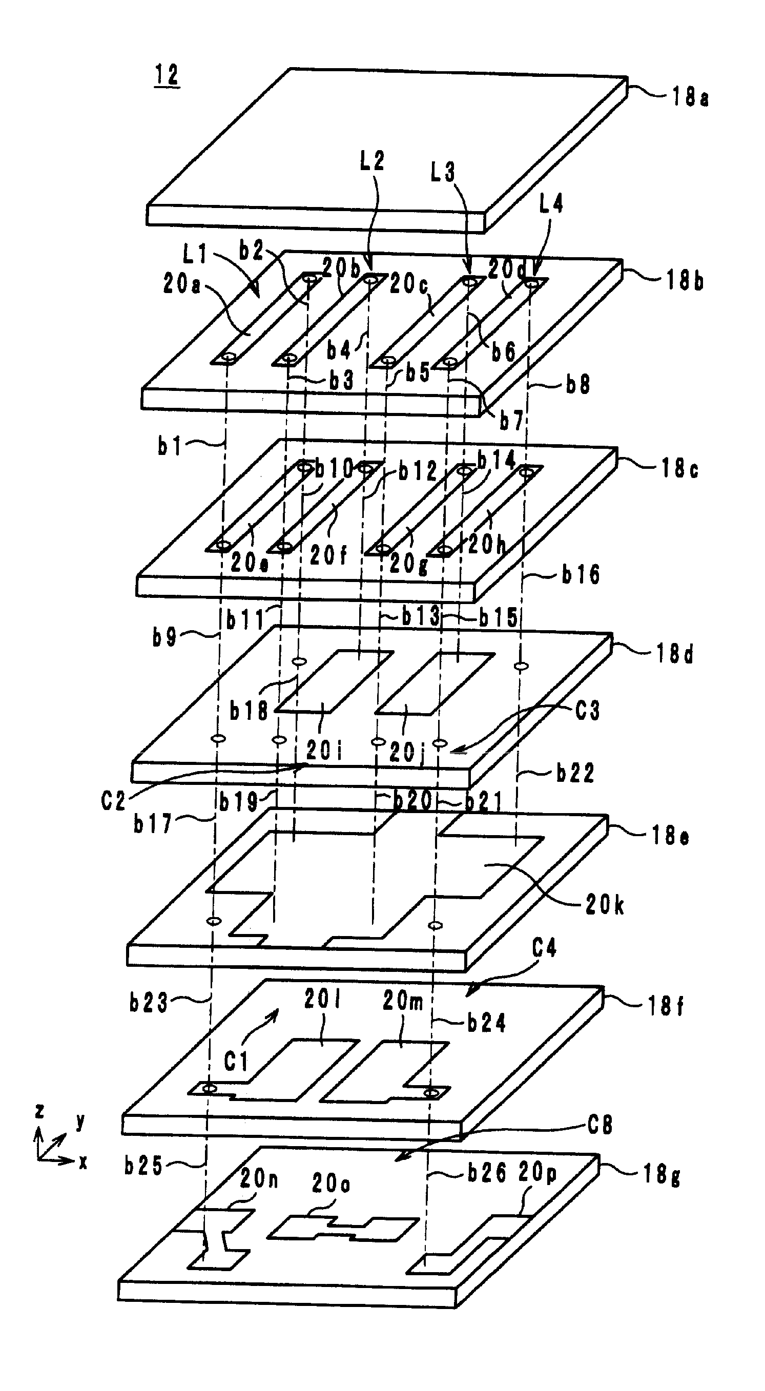
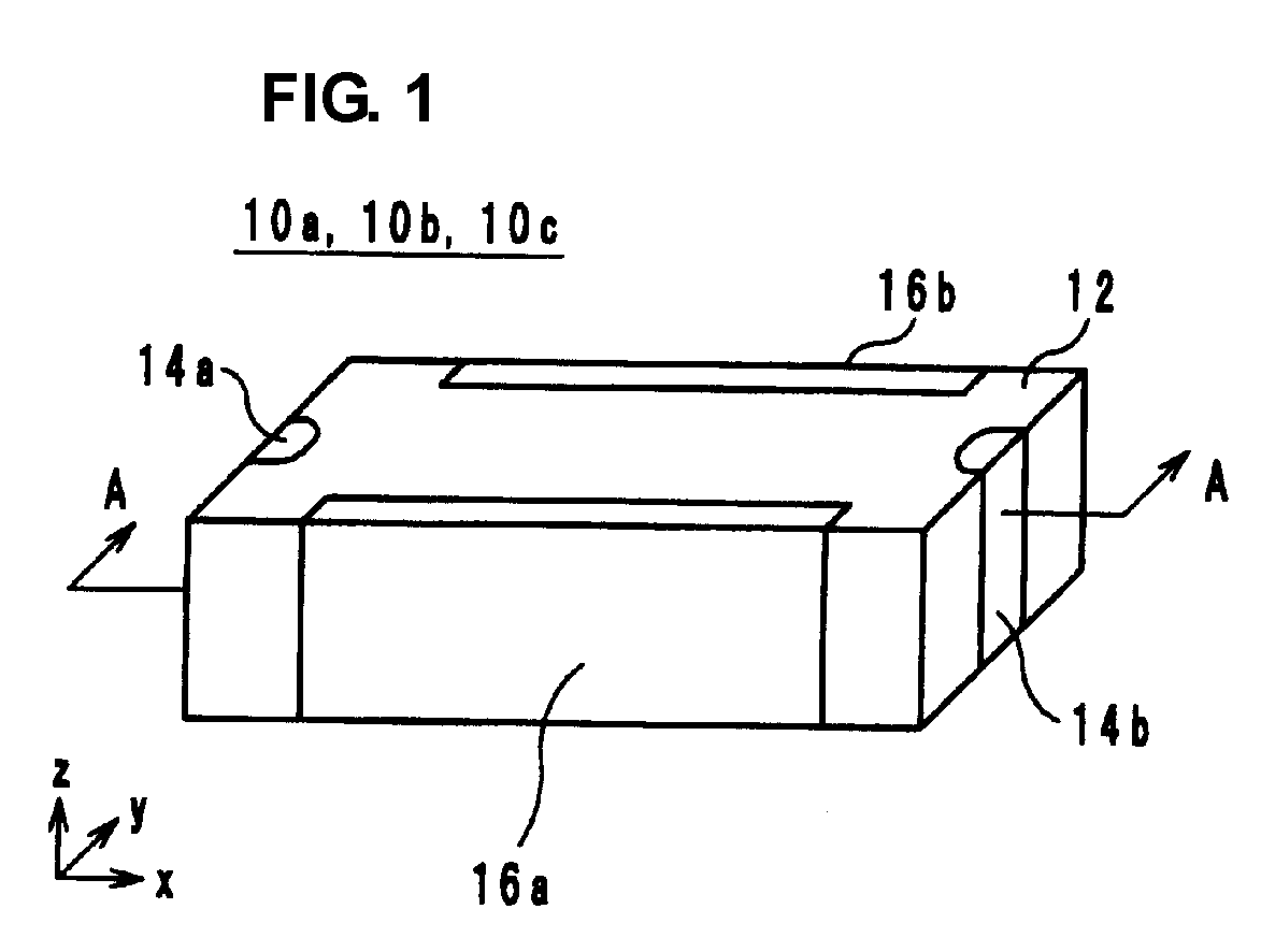
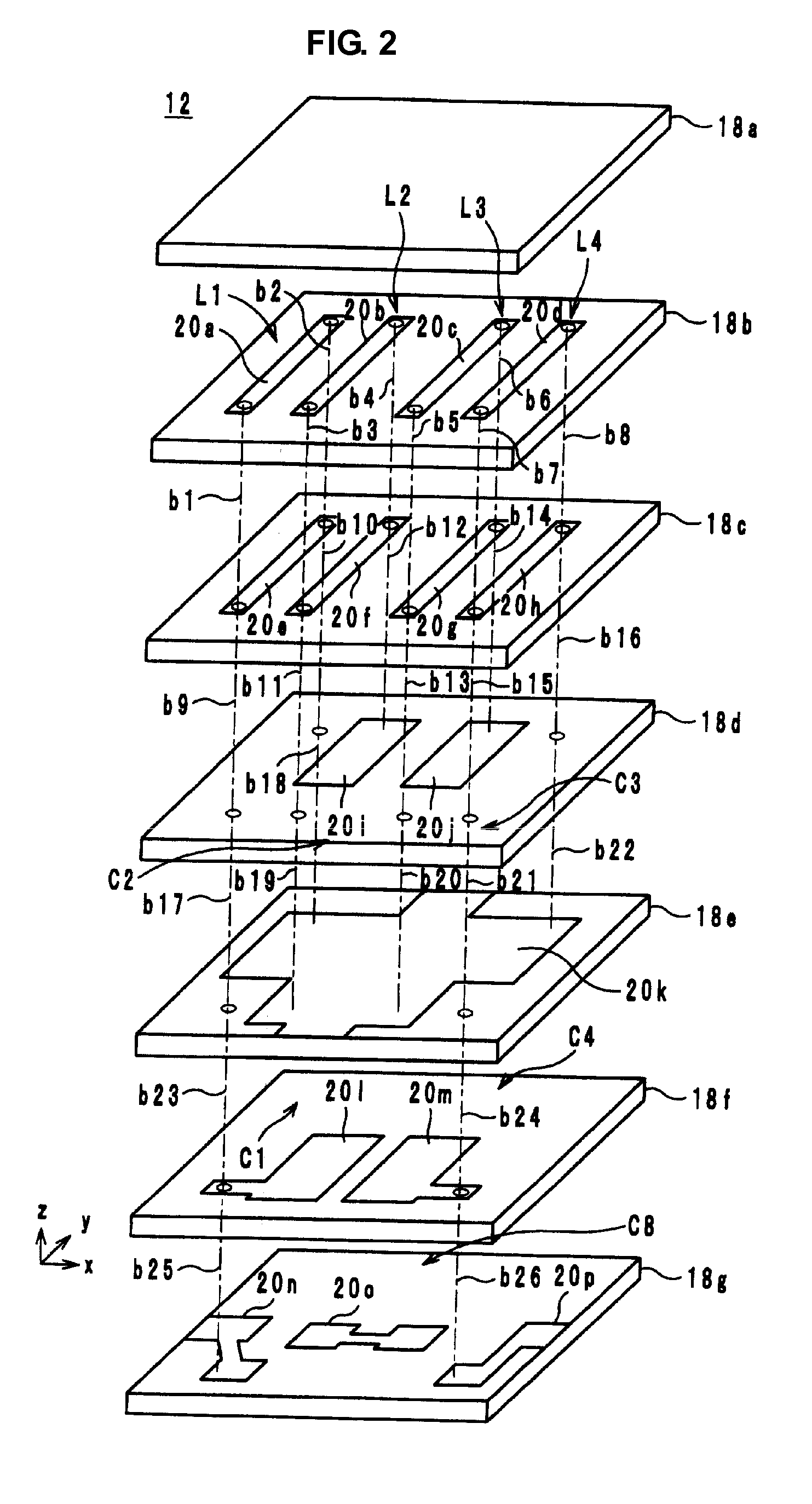
[0022]A configuration of an electronic component according to a first preferred embodiment will be described with reference to the drawings. FIG. 1 is an external perspective view of an electronic component 10a, 10b, or 10c according to a preferred embodiment of the present invention. FIG. 2 is an exploded perspective view illustrating a laminated body 12 of the electronic component 10a, 10b, or 10c according to a preferred embodiment of the present invention. FIG. 3 is an equivalent circuit diagram of the electronic component 10a, 10b, or 10c according to a preferred embodiment of the present invention. FIG. 4 illustrates a cross section of the electronic component 10a according to a first preferred embodiment, the cross section being taken along line A-A of FIG. 1. In FIG. 1 to FIG. 4, a stacking direction of the laminated body 12 is defined as a z-axis direction, a long-side direction of the laminated body 12 is defined as an x-axis direction, and a short-side direction of the la...

second preferred embodiment

[0053]A configuration of an electronic component according to a second preferred embodiment will be described with reference to the drawings. The external perspective view, the exploded perspective view, and the equivalent circuit diagram of FIG. 1 to FIG. 3 are used again for the description. FIG. 6 illustrates a cross section of the electronic component 10b according to the second preferred embodiment, the cross section being taken along line A-A of FIG. 1. In FIG. 6, a stacking direction of the laminated body 12 is defined as a z-axis direction, a long-side direction of the laminated body 12 is defined as an x-axis direction, and a short-side direction of the laminated body 12 is defined as a y-axis direction. The x-axis direction, the y-axis direction, and the z-axis direction are orthogonal to each other.

[0054]As illustrated in FIG. 4 and FIG. 6, the electronic component 10a and the electronic component 10b differ in the shape of the conductor layers 20a to 20h. Specifically, w...


PUM

PropertyMeasurementUnit
Thicknessaaaaaaaaaa
Shapeaaaaaaaaaa
Electrical conductoraaaaaaaaaa

Abstract

An electronic component that reduces resistance and prevents occurrence of an edge effect, includes a laminated body formed by stacking insulator layers. Conductor layers are linear conductors, and define coils included in the laminated body. The conductor layers face each other, with the insulator layer interposed therebetween, and allow signals of substantially the same phase to pass therethrough. The conductor layers define regions, each having a shape which decreases in thickness in the z-axis direction with increasing distance from a center thereof in a line width direction.

Description

BACKGROUND OF THE INVENTION[0001]1. Field of the Invention[0002]The present invention relates to an electronic component and a method for making the electronic component. In particular, the present invention relates to an electronic component including coils and a method for making the electronic component.[0003]2. Description of the Related Art[0004]A high-frequency coil described in Japanese Unexamined Patent Application Publication No. 5-36533 includes a helical coil in a multilayer substrate. The helical coil is formed by connecting a plurality of coil patterns. The coil patterns are composed of more than one set of two coil patterns having the same shape. The two coil patterns having the same shape are connected in parallel such that they are at the same potential. This reduces resistance of the helical coil.[0005]In the high-frequency coil described above, the coil patterns are rectangular in cross section. Applying a high-frequency signal to the coil patterns of rectangular c...

Claims


Application Information

Patent Timeline
IPC IPC(8): H01F5/00H01F41/00
CPCH01F17/0013H01F2017/0026H03H7/0115Y10T29/4902H03H7/1775H03H2001/0085H03H7/1708
Inventor MATSUSHITA, YOSUKETANIGUCHI, TETSUOTERAMOTO, MASAHIRO
Owner MURATA MFG CO LTD
Learn More