
Ceramic element inlaid with at least one metallic decoration

a ceramic element and metallic technology, applied in the field of ceramic elements inlaid with at least one metallic decoration, can solve problems such as difficulty in reading decoration

Active Publication Date: 2011-10-27
OMEGA SA
View PDF9 Cites 34 Cited by
  • Summary
  • Abstract
  • Description
  • Claims
  • Application Information

AI Technical Summary

Benefits of technology

[0004]It is an object of the present invention to overcome all or part of the aforementioned drawbacks, while maintaining the advantage of mechanical resistance and adding the advantage of improved visual quality.
[0023]the method includes a final step g) for the deposition of a substantially transparent layer to protect the decorations from ageing, such as, for example, a layer of silicon nitride.

Problems solved by technology

However, this configuration may make it difficult to read the decoration because of the transmitted colouring of the deposit fades but also because of the lack of difference in colour between the sapphire and the deposit.

Method used


Image

  • Ceramic element inlaid with at least one metallic decoration
  • Ceramic element inlaid with at least one metallic decoration
  • Ceramic element inlaid with at least one metallic decoration

Examples


first embodiment

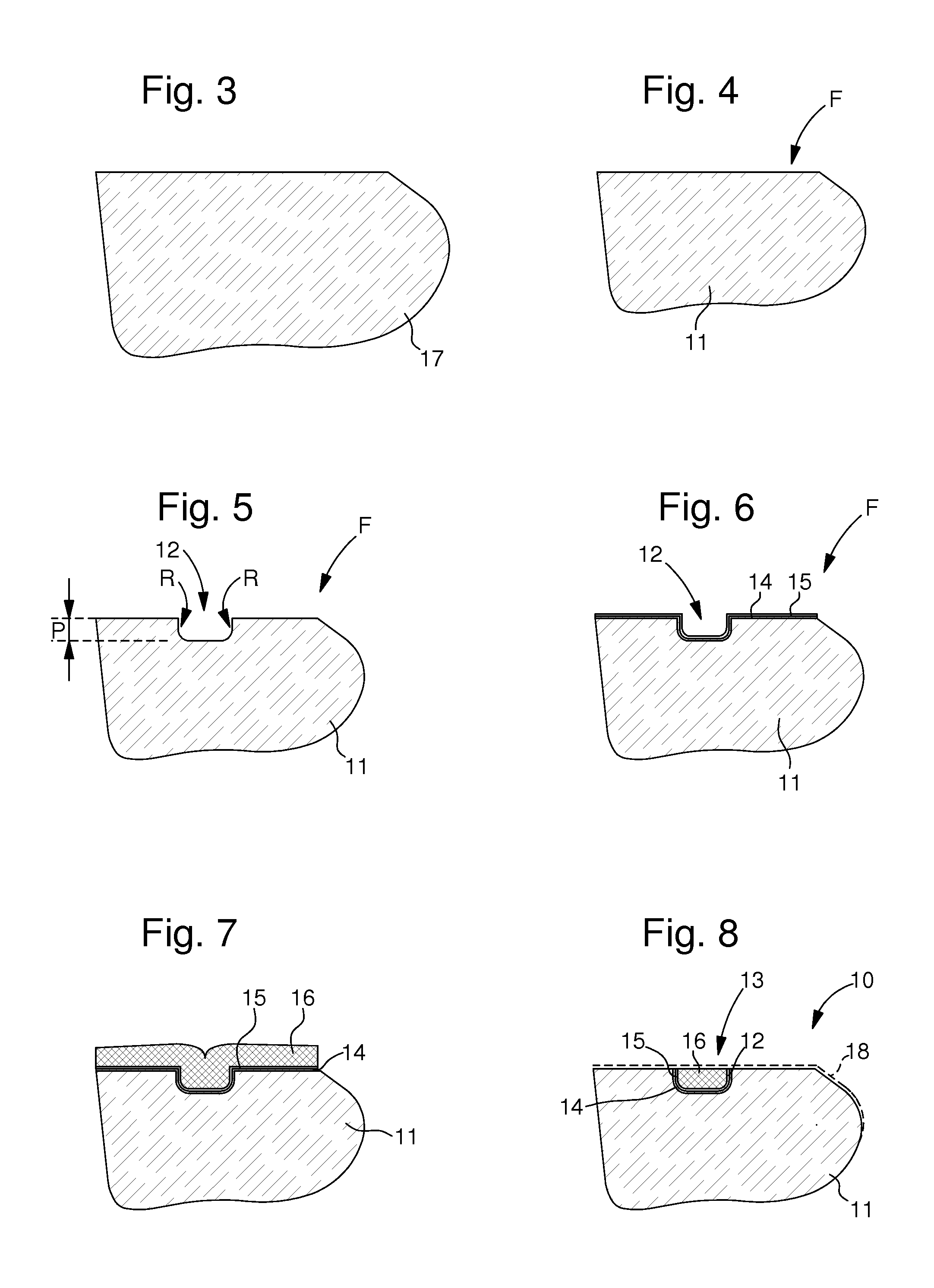
[0042]In a first embodiment, visible in a single line in FIG. 9, the third step 24 of method 21 consists in coating face F using a wet method, such as, for example chemical auto-catalytic or electroless plating. It is thus possible to deposit, for example, a nickel-phosphorus chemical layer which perfectly adheres to ceramic body 11 and which forms a very good adhesion layer for the subsequent step 26.

second embodiment

[0043]In a second embodiment, seen in double lines in FIG. 9, the third step 25 of method 21 consists in coating face F using a dry method, such as for example a vapour phase deposition. It is therefore possible to deposit, for example, a Cr, Cr2N, TiN, TiW, Ni, NiP, Cu, Ti or Zr layer that perfectly adheres to ceramic body 11 and which forms a very good adhesion layer for the subsequent step 26.

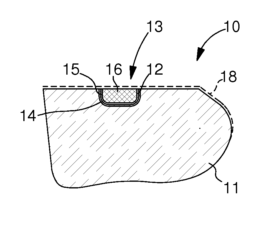
[0044]Whichever embodiment is selected, method 21 continues with a fourth step 26 for depositing a second electrically conductive layer 15 with a thickness of approximately 50 nm over the entire face F, i.e. including in recesses 12, so as to cover first layer 14 so as to offer an optimised surface for the electroplating step 27. As explained above, optimisation applies to the adherence, good electrical conductivity and colour close to galvanic deposition 16.

[0045]Consequently, this layer 15 may, for example, be made of gold and / or copper and / or silver and / or indium and / or platinum and / or pa...


PUM

PropertyMeasurementUnit
Nanoscale particle sizeaaaaaaaaaa
Electrical conductivityaaaaaaaaaa
Transparencyaaaaaaaaaa

Abstract

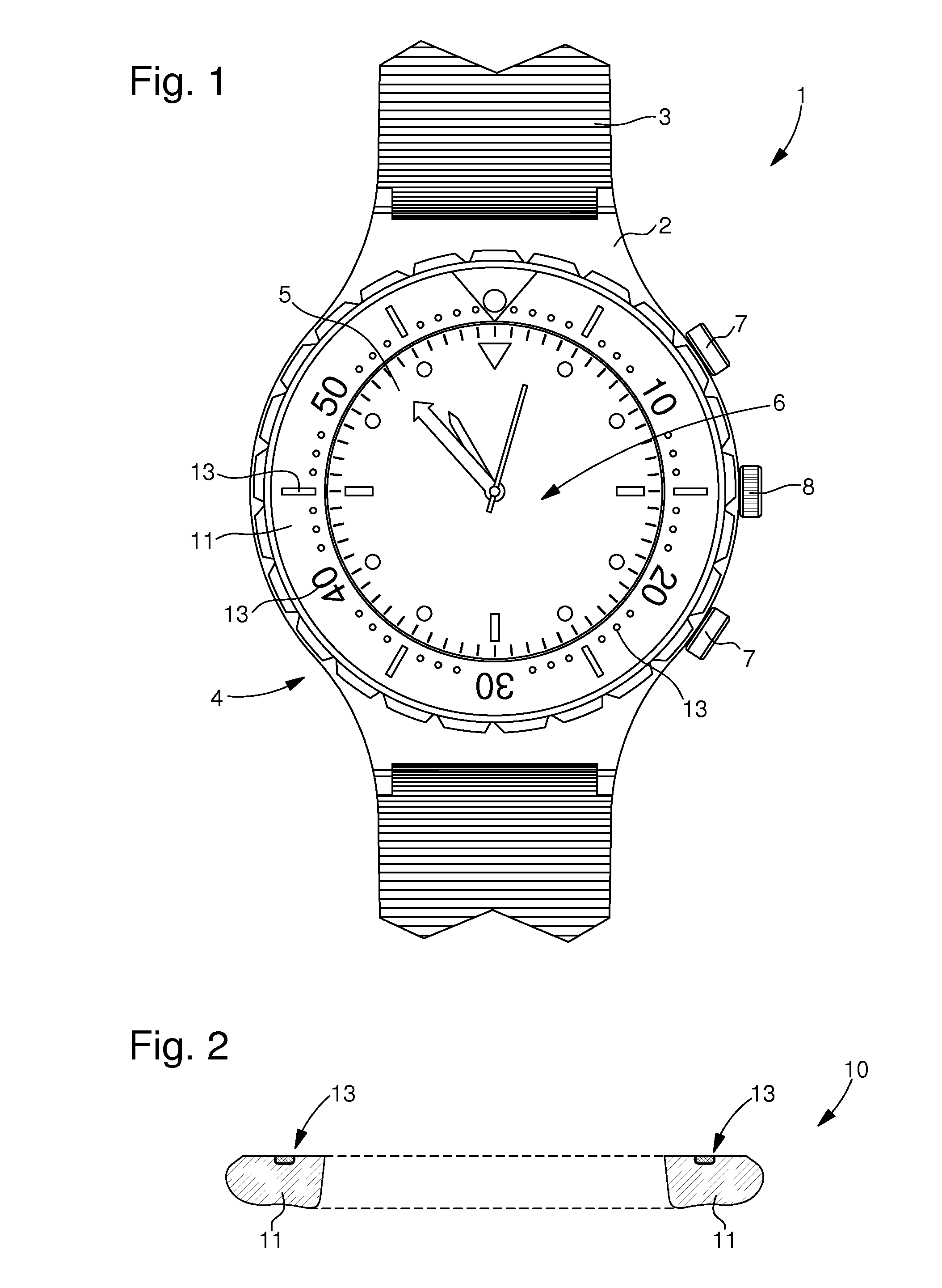
The invention relates to an inlaid ceramic decoration (10) including a ceramic body (11) that has at least one recess (12) forming the pattern for a decoration (13). According to the invention, said at least one recess is entirely filled by first and second electrically conductive layers (14, 15) of approximately 50 nm and a metallic galvanic plating (16) so as to form a ceramic element (10) inlaid with at least one metallic decoration (13) with improved visual rendering.The invention also relates to the method of manufacturing the inlaid ceramic element.The invention concerns the field of decorated ceramic parts.

Description

[0001]This application claims priority from European Patent Application No. 10160893.3 filed Apr. 23, 2010, the entire disclosure of which is incorporated herein by reference.FIELD OF THE INVENTION[0002]The invention relates to a ceramic element inlaid with at least one metallic decoration and more specifically an element of this type that is intended to be mounted in a timepiece.BACKGROUND OF THE INVENTION[0003]It is known to form watch bezels at least partially made of synthetic sapphire in order to show, through transparency, a deposit plated in a recess underneath the bezel, for example, forming a scale or a brand name. This configuration has the advantage of protecting the deposit from any mechanical degradation by totally covering it with the sapphire part. However, this configuration may make it difficult to read the decoration because of the transmitted colouring of the deposit fades but also because of the lack of difference in colour between the sapphire and the deposit.SU...

Claims


Application Information

Patent Timeline
IPC IPC(8): C25D5/54
CPCB44C1/26C04B41/009C04B41/52C04B41/90G04B19/18G04B19/28C04B35/00C04B35/48C04B41/4541C04B41/4572C04B41/5144C04B41/4529C04B41/5133C04B41/522C04B41/5062C04B41/5127C04B41/51C04B41/4568C04B41/4576C04B41/5066C25D5/10C25D5/627C23C14/06C23C18/31C23C28/00C23F1/02
Inventor GROSSENBACHER, PASCALCAILLAUD, MICHELNETUSCHILL, ALEXANDRE
Owner OMEGA SA
Learn More