
Etching processing method

Active Publication Date: 2011-10-06
TOKYO ELECTRON LTD
View PDF5 Cites 12 Cited by
  • Summary
  • Abstract
  • Description
  • Claims
  • Application Information

AI Technical Summary

Benefits of technology

In view of the above, the present invention provides an etching processing method capable of preventing deformation of a pattern even when it has a high aspect ratio thereof.
With the present invention, there is provided an etching processing method capable of preventing deformation of a pattern in spite of a high aspect ratio thereof.

Problems solved by technology

When the hole has an aspect ratio of about 30 or higher, it is difficult to prevent the hole from being deformed even by using the above-described technique.

Method used


Image

  • Etching processing method
  • Etching processing method
  • Etching processing method

Examples


first embodiment

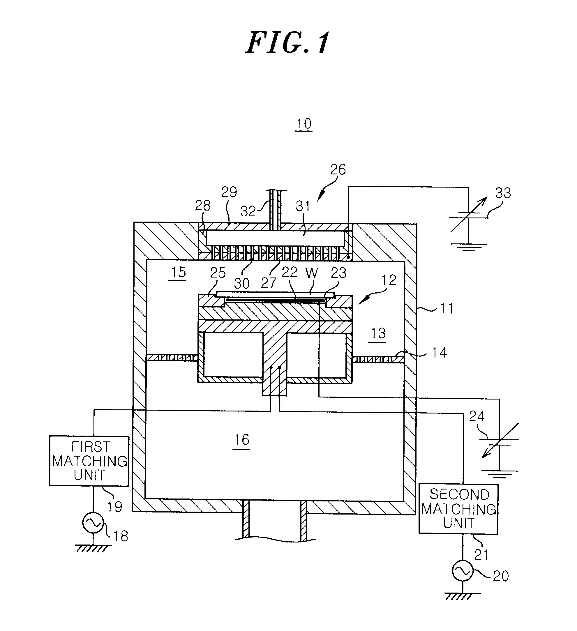
First, a substrate processing apparatus for performing an etching processing method in accordance with a first embodiment of the present invention will be described.

FIG. 1 schematically shows the configuration of the substrate processing apparatus for performing the etching processing method of the present embodiment. This substrate processing apparatus performs a plasma etching process on a wafer for a semiconductor device (hereinafter, referred simply to as “wafer”) as a substrate.

Referring to FIG. 1, a substrate processing apparatus 10 includes a chamber 11 for accommodating therein a wafer W having a diameter of, e.g., about 300 mm, and a cylindrical susceptor 12 for mounting thereon the wafer W is disposed in the chamber 11. In the substrate processing apparatus 10, a side exhaust passageway 13 is defined by an inner sidewall of the chamber 11 and a side surface of the susceptor 12. A gas exhaust plate 14 is provided in the side exhaust passageway 13.

The gas exhaust plate 14 is...

second embodiment

Hereinafter, an etching processing method in accordance with a second embodiment of the present invention will be described in detail.

The configuration and the operation of the second embodiment are basically the same as those of the first embodiment. Therefore, the description of the same configuration and operation will be omitted, and only the difference will be explained.

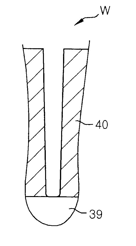
FIG. 9 is a cross sectional view schematically showing a structure of a part of a wafer processed by the etching processing method of the present embodiment.

Referring to FIG. 9, a wafer Wa includes a silicon portion 39 serving as a base portion, an SiO2 film 40 (etching target film) formed on the silicon portion 39 and having a thickness of, e.g., about 2600 nm, a polysilicon film 58 formed on the SiO2 film 40, and a residue film 59 made of SiO2 and formed on the polysilicon film 58. The polysilicon film 58 and the residue 59 have a hole 60 for exposing the SiO2 film 40. The residue film 59 is formed of residues...


PUM


Abstract

An etching processing method for etching a substrate formed with a target film and a mask film is performed in a substrate processing apparatus including a first and a second power supply for respectively supplying a higher and a lower high frequency power to a processing space and a mounting table, and a DC power supply for supplying a DC power to an electrode. The method includes a modification step for modifying a shape of a pattern formed on the mask film; and an etching step for etching the target film by using the mask film. The mask film is etched by the plasma in the modification step. Further, in the etching step, the DC power is applied to the electrode and the lower high frequency power is applied to the mounting table in a pulse wave form in which a higher and a lower power level are repeated.

Description

FIELD OF THE INVENTIONThe present invention relates to an etching processing method for forming a hole or the like having a high aspect ratio.BACKGROUND OF THE INVENTIONIn a semiconductor device manufactured from a semiconductor wafer by using a plasma etching apparatus, it is required to form a pattern having a relatively large depth compared to a diameter thereof, e.g., a hole having a high aspect ratio.In order to form a hole having a high aspect ratio, a target film needs to be sputtered especially by positive ions in the plasma. In that case, as shown in FIG. 12, positive ions 122 remain at a bottom portion of a hole 121 formed in a target film 120 and electrically prevent succeeding positive ions 123 from approaching the bottom portion of the hole 121, which causes the path of the positive ions 123 inside the hole 121 to be changed. Accordingly, the problem such as deformation of the hole 121 or the like may occur.For that reason, there has been developed a technique for intro...

Claims


Application Information

Patent Timeline
IPC IPC(8): H01L21/3065
CPCH01J37/32091H01J37/32165H01L21/0273H01L21/32137H01L21/31122H01L21/31138H01L21/31144H01L21/31116
Inventor MOCHIKI, HIROMASAOKAMOTO, SHINNISHIJIMA, TAKASHIYAMAZAKI, FUMIO
Owner TOKYO ELECTRON LTD
Learn More