
Amorphous silicon solar cells

a solar cell and amorphous silicon technology, applied in the field of materials science, can solve the problems of microscopic explanation, inability to practically mitigate the swe of amorphous silicon, and the deformation of amorphous silicon under light exposure, and achieve the effects of suppressing bond rotation, reducing the swe, and reducing the sw

Inactive Publication Date: 2011-09-22
RGT UNIV OF CALIFORNIA
View PDF10 Cites 5 Cited by
  • Summary
  • Abstract
  • Description
  • Claims
  • Application Information

AI Technical Summary

Benefits of technology

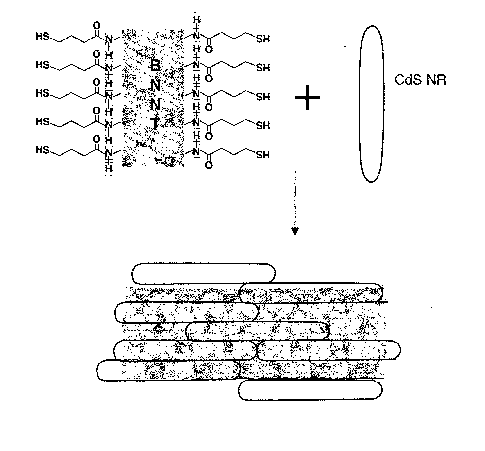
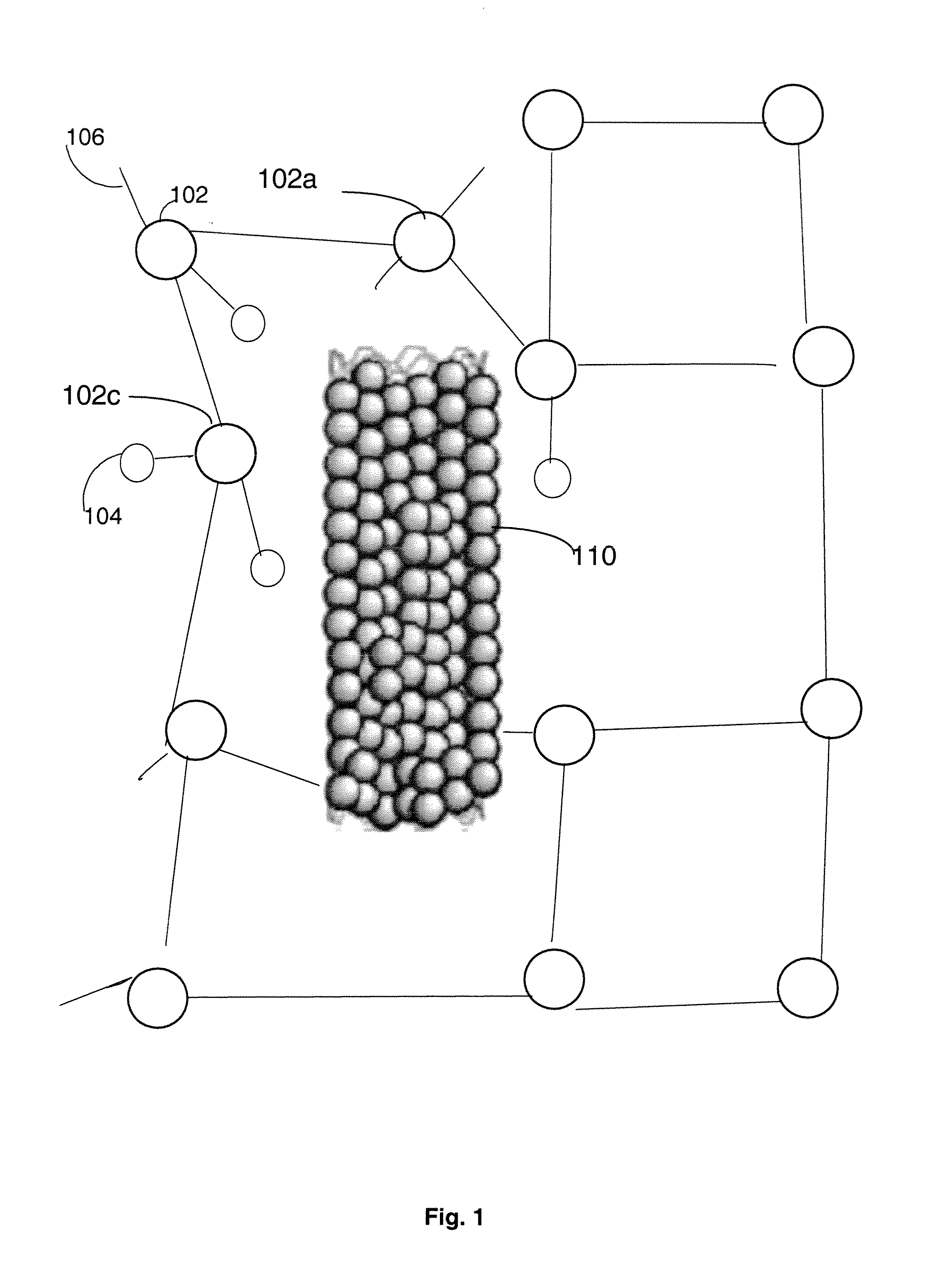
[0012]Accordingly, the present invention provides novel strategies for mitigating the SWE in amorphous silicon. In a first embodiment, materials are provided that affect the energetics of bond rotations. Specifically, these materials result in a more rigid network, such that bond rotations are suppressed. In one aspect of this embodiment, alloys are used to increase the rigidity of the bond network. The term “alloys” is intended to include composite materials where nanocrystals and nanoparticles such as fullerenes of various sizes are included in the a-Si. Thus, nanoparticles, e.g., nanotubes or nanospheres, or nanocrystals are embedded in the in the material to increase the rigidity of the bond network.
[0013]In a third embodiment, methods are used to reduce the internal stress in the a-Si:H (amorphous silicon). In one aspect of this embodiment, anisotropic pressure is used to control bond rotations and the resulting strained regions of bonds, thus improving the performance of the device. Pressure may be induced, for example, by flexing the substrate upon which the amorphous silicon is grown. Alternatively, pressure may be externally applied, such as in the form of a compression sandwich. In a similar vein, nanoscale features in the material may be used that allow stress to be relieved.

Problems solved by technology

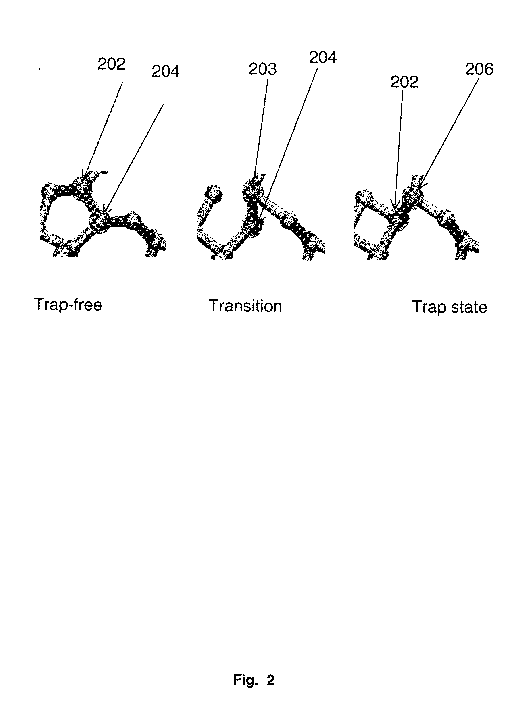
However, amorphous silicon degrades under exposure to light, an effect that so far cannot be practically mitigated and that has remained without microscopic explanation since its discovery in 1977 (Staebler-Wronski Effect, WSE).
This effect has greatly limited the use of a-Si:H in a broad range of applications, particularly in solar cells, where it is responsible for a decrease in the energy conversion efficiency of 30%.
Amorphous silicon on the other hand, could be more attractive due to its lower costs and thinner, lighter panels, but its efficiency after SWE degradation is too low, requiring a large area panel to power a home.
Mitigating the SWE would boost the efficiency of a-Si:H solar cell enough to make them much more attractive as sources of residential and commercial power, but without a microscopic explanation of the effect, efforts at mitigation are mostly driven by trial and error.

Method used


Image

  • Amorphous silicon solar cells
  • Amorphous silicon solar cells
  • Amorphous silicon solar cells

Examples


Embodiment Construction

Definitions

[0025]The term “hydrogenated amorphous silicon” is used in its conventional sense. That is, amorphous silicon refers to the non-crystalline allotropic form of silicon. Silicon is a four-fold coordinated atom that is normally tetrahedrally bonded to four neighboring silicon atoms. In crystalline silicon this tetrahedral structure is continued over a large range, forming a well-ordered lattice (crystal). In amorphous silicon this long range order is not present and the atoms form a continuous random network. Not all the atoms within amorphous silicon are four-fold coordinated. If desired, the material can be passivated by hydrogen, which bonds to the dangling bonds and can reduce the dangling bond density by several orders of magnitude. Hydrogenated amorphous silicon (a-Si:H) has a sufficiently low amount of defects to be used within devices. Hydrogenated amorphous silicon (a-Si:H) is widely applied commercially in thin film solar cells by means of plasma enhanced chemical ...


PUM

PropertyMeasurementUnit
diameteraaaaaaaaaa
diameteraaaaaaaaaa
diameteraaaaaaaaaa

Abstract

The present invention provides novel strategies for mitigating the Staebler-Wronski Effect (SWE), that is, the light induced degradation in performance of photoconductivity in amorphous silicon. Materials according to the present invention include alloys or composites of amorphous silicon which affect the elasticity of the materials, amorphous silicon that has been grown on a flexed substrate, compression sandwiched comprising amorphous silicon, and amorphous silicon containing nanoscale features that allow stress to be relieved. The composites are formed with nanoparticles such as nanocrystals and nanotubes. Preferred are boron nitride nanotubes (BNNT) including those that have been surface modified.

Description

CROSS-REFERENCE TO RELATED APPLICATIONS[0001]The present application claims priority from U.S. Provisional Patent Application No. 61 / 091,379, filed on Aug. 23, 2008, which is hereby incorporated by reference in its entirety.STATEMENT OF GOVERNMENTAL SUPPORT[0002]This invention was made with U.S. Government support under Contract Number DE-AC02-05CH11231 between the U.S. Department of Energy and The Regents of the University of California for the management and operation of the Lawrence Berkeley National Laboratory. This invention was also made with U.S. Government support under the auspices of the National Science Foundation by the University of California Berkeley under Grant No. 0425914. The U.S. Government has certain rights in this invention.REFERENCE TO SEQUENCE LISTING, COMPUTER PROGRAM, OR COMPACT DISK[0003]None.BACKGROUND OF THE INVENTION[0004]1. Technical Field[0005]The present invention relates to the field of materials science, and in particular to amorphous silicon mater...

Claims


Application Information

Patent Timeline
Patent Type & Authority Applications(United States)
IPC IPC(8): H01L31/0384H01L31/20H01L51/42H01B1/04B82Y30/00B82Y40/00B82Y99/00
CPCH01L31/03767Y02E10/50H01L31/202H01L31/03921Y02P70/50
Inventor GROSSMAN, JEFFREY C.ZETTL, ALEXANDER K.WAGNER, LUCAS
Owner RGT UNIV OF CALIFORNIA
Learn More