Photoelectric conversion device
- Summary
- Abstract
- Description
- Claims
- Application Information
AI Technical Summary
Benefits of technology
Problems solved by technology
Method used
Image

Examples
example 1
[0076]Example 1 relates to the photoelectric conversion device according to an embodiment of the present invention, particularly to a dye-sensitized solar cell.
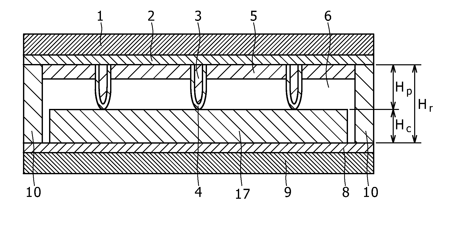
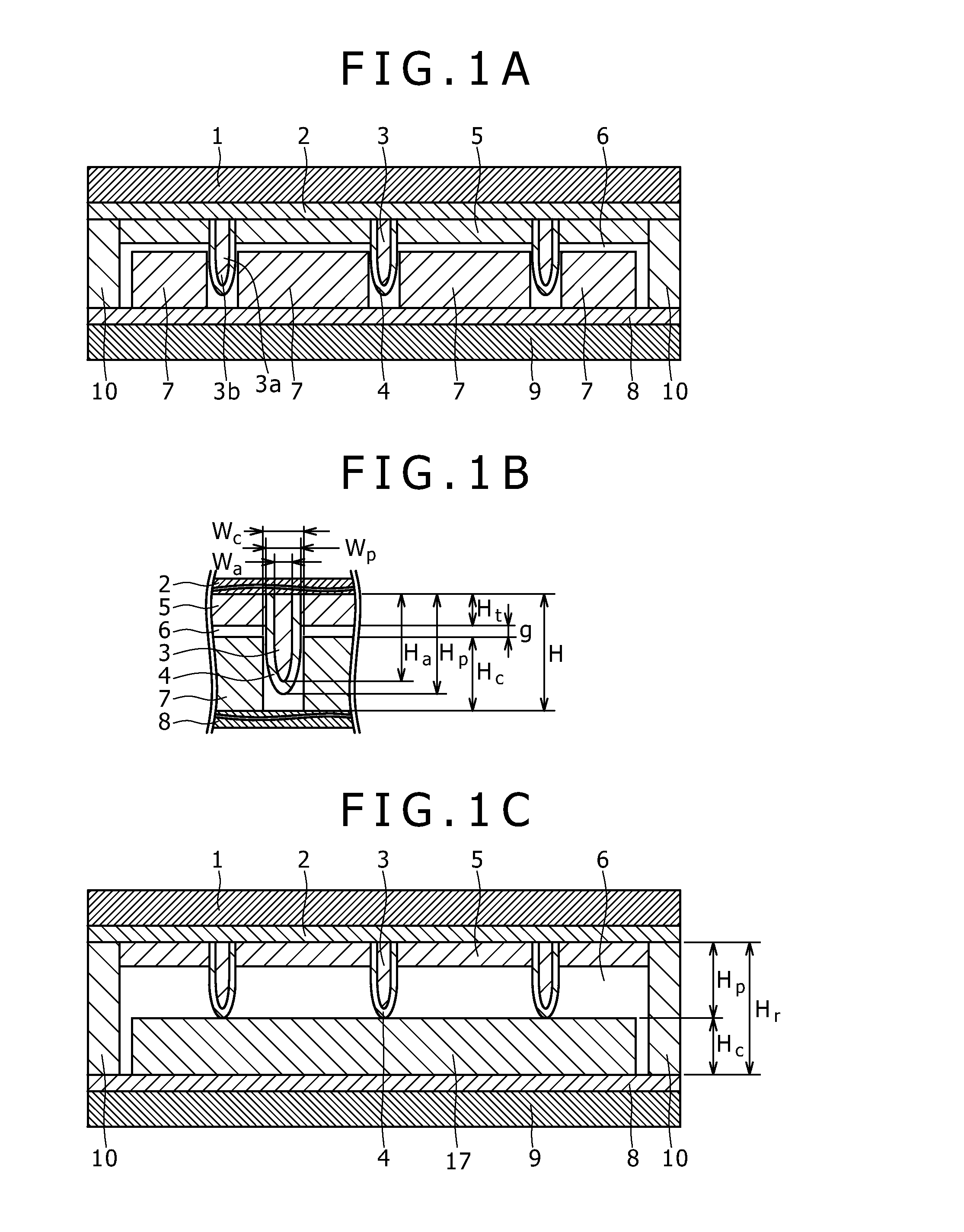
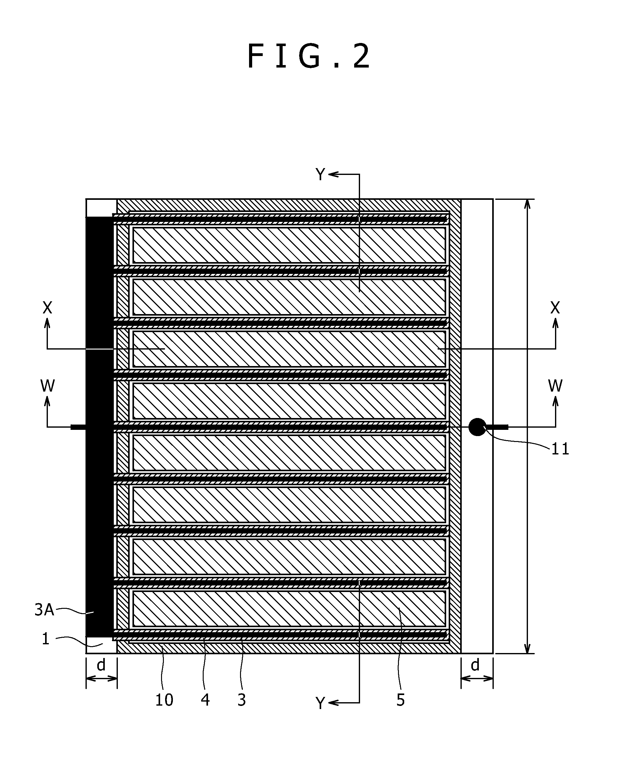
[0077]A schematic partial sectional view of a photoelectric conversion device according to Example 1 of the present invention is shown in FIGS. 1A to 1C, and an enlarged schematic partial sectional view of a part of the photoelectric conversion device of Example 1 is shown in FIG. 1B. Also, a schematic partial sectional view of a photoelectric conversion device according to Comparative Example 1A is shown in FIG. 1C. In addition, a schematic plan view of the photoelectric conversion device of Example 1 is shown in FIG. 2, and projection views obtained by projection of formation patterns of layers constituting the photoelectric conversion device of Example 1 are shown in FIGS. 3A and 3B, wherein FIG. 3A is a view obtained by projecting the formation patterns of oxide semiconductor layers, current collectors and a sealing layer...
example 2
[0142]In Example 2, which is a modification of Example 1, the relation between photoelectric conversion efficiency and the distance (gap) g between the oxide semiconductor layer and the catalyst layer was examined. In photoelectric conversion devices in Example 2, the distance g between the oxide semiconductor layer 5 and the catalyst layer 7 was variously changed from 2 μm to 86 μm. Further, attendant on the change in the distance g, optimization of other distances and the like in the photoelectric conversion devices was contrived. In such a way, photoelectric conversion devices for tests were fabricated on an experimental basis.
[0143]Variations in open circuit voltage VOC, short-circuit current density JSC, fill factor FF, internal resistance RS, and photoelectric conversion efficiency, with various changes in the distance g between the oxide semiconductor layer and the catalyst layer, are shown in FIGS. 15A, 15B, 16A, 16B, and 17, respectively. In each of FIGS. 15A, 15B, 16A, 16B...
PUM
 Abstract
Description
Claims
Application Information
 - R&D
- Intellectual Property
- Life Sciences
- Materials
- Tech Scout
- Unparalleled Data Quality
- Higher Quality Content
- 60% Fewer Hallucinations
Browse by: Latest US Patents, China's latest patents, Technical Efficacy Thesaurus, Application Domain, Technology Topic, Popular Technical Reports.
© 2025 PatSnap. All rights reserved.Legal|Privacy policy|Modern Slavery Act Transparency Statement|Sitemap|About US| Contact US: help@patsnap.com