
Semiconductor device

a technology of semiconductors and components, applied in semiconductor devices, semiconductor/solid-state device details, cooling/ventilation/heating modifications, etc., can solve the problems of increasing assembly man-hour and increasing the number of components

Inactive Publication Date: 2011-09-08
KEIHIN CORP
View PDF34 Cites 20 Cited by
  • Summary
  • Abstract
  • Description
  • Claims
  • Application Information

AI Technical Summary

Benefits of technology

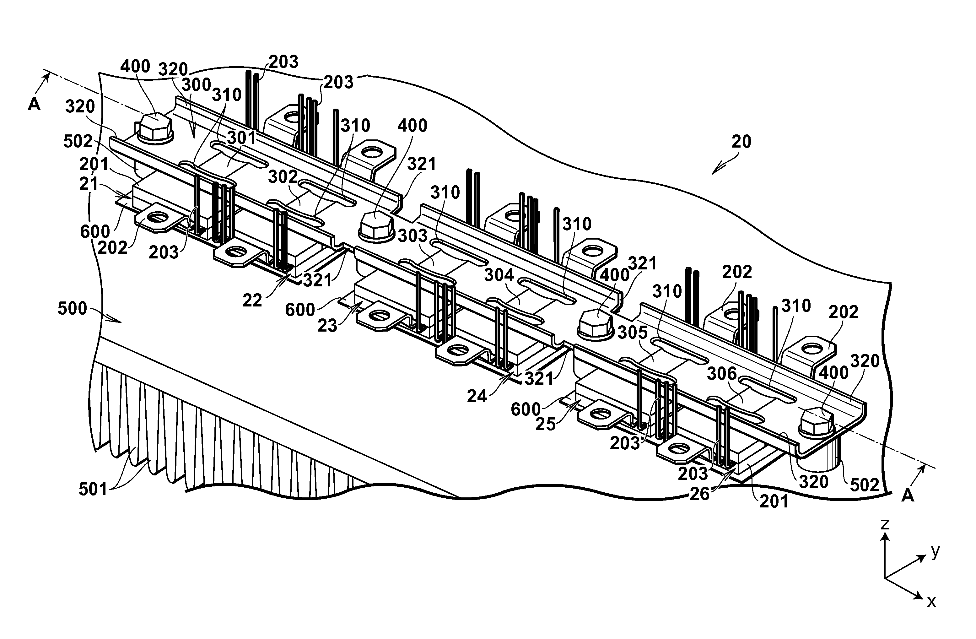
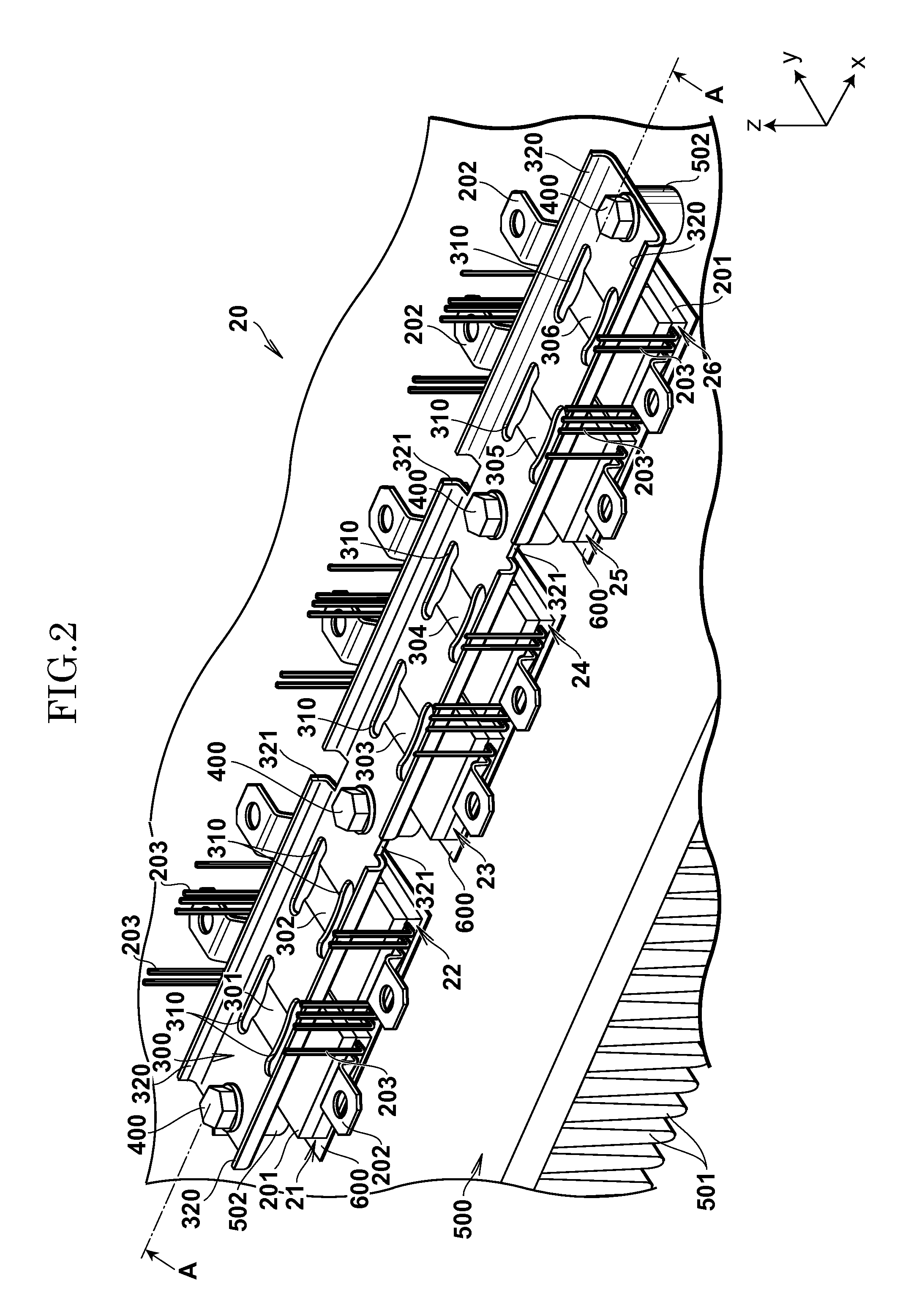
The present invention provides a semiconductor device that reduces the number of component parts with a simplified structure. The invention includes a power module, a cooling member, and a mounting member. The mounting member is integrally formed with a spring portion protruding in part therebetween and having elasticity, allowing the power module to be mounted on the cooling member under a state where one surface of the power module is caused to face the cooling member and the spring portion is pressed against the other surface of the power module in opposition to the one surface. The invention also includes a through-hole provided in a part of a circumferential portion surrounding the spring portion, which simplifies the fabrication of the spring portion. The invention further includes a fastening aperture and cutout portions formed by removing parts of the pair of flange portions, which allows for a uniform pressing force and prevents undesired fastening force from acting on the power module. Overall, the invention simplifies the structure of the semiconductor device and reduces the number of component parts.

Problems solved by technology

This results in a tendency of causing an increase in the number of component parts with the occurrence of a complicated structure.
With such structures, further, the spring member is sandwiched between the power module and the pressing member, under which a need arises to inevitably perform work of assembling the power modules onto the heat sink while causing the pressing members to be intervened therebetween as kept depressed, resulting in another tendency of causing increased assembling man-hour.

Method used


Image

  • Semiconductor device
  • Semiconductor device
  • Semiconductor device

Examples


Embodiment Construction

[0028]Now, a semiconductor device of an embodiment according to the present invention will be described below in detail with reference to the accompanying drawings. Throughout the drawings, an x-axis, a y-axis and a z-axis represent a three-axis orthogonal coordinate system with a direction of the x-axis representing a longitudinal direction, a direction of the y-axis representing a lateral direction and a direction of the z-axis representing a vertical direction.

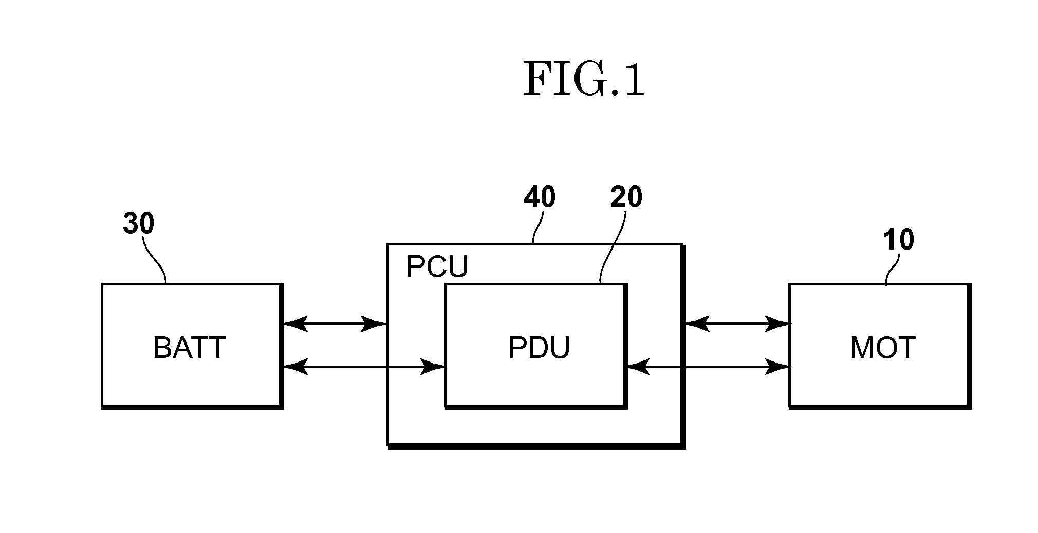
[0029]First, a structure of a control apparatus for a vehicle, to which the semiconductor device of the present embodiment is applied, will be described below in detail with reference to FIG. 1. In addition, the semiconductor device of the present embodiment will be described below with reference to a power drive unit by way of example.

[0030]FIG. 1 is a block diagram showing a structure of a control apparatus, with its related devices, for the vehicle to which the semiconductor device of the present embodiment is applied.

[0...


PUM


Abstract

A semiconductor device is provided with a power module capable of supplying an alternate current to a load, while a direct current is supplied from a battery to the power module for conversion into the alternate current, a cooling member capable of radiating heat generated by the power module, and a mounting member, integrally formed with a spring portion protruding in part therefrom and having elasticity, which allows the power module to be mounted on the cooling member under a state where one surface of the power module is caused to face the cooling member and the spring portion is pressed against the other surface of the power module in opposition to the one surface thereof.

Description

BACKGROUND OF THE INVENTION[0001]The present invention relates to a semiconductor device and, more particularly, to a semiconductor device having a mounting member with which a functional device, such as a power module, is mounted on a cooling member.[0002]In recent years, a hybrid vehicle provided with a drive-force source composed of an engine, such as an internal combustion engine, and a motor such as an electric motor, have been widely spread in use. Such a hybrid vehicle has a power drive unit through which a direct current, supplied from a battery, is converted to an alternate current for supply to the motor whereas an alternate current, resulting from regenerative operation of the motor, is converted to a direct current for storage in the battery.[0003]The power drive unit is provided with a power module for performing such DC / AC conversion and AC / DC conversion. Such a power drive unit employs a relatively large current and, hence, a power module, incorporating so-called powe...

Claims


Application Information

Patent Timeline
Patent Type & Authority Applications(United States)
IPC IPC(8): H05K7/20
CPCH05K7/20H01L2924/00H01L2924/0002H01L23/4006H05K7/209H02M7/003H01L23/4093
Inventor KADOMOTO, KEIKUDO, DAIKINAKAMURA, TAKESHINAKADE, HIROYUKI
Owner KEIHIN CORP
Learn More