Integrated circuit connection device

Active Publication Date: 2011-07-21
EM MICROELECTRONIC-MARIN
View PDF7 Cites 1 Cited by
  • Summary
  • Abstract
  • Description
  • Claims
  • Application Information

AI Technical Summary

Benefits of technology

One advantage of the present invention is that the device allows improved protection of the integrated circuit. Indeed, by being capable of operating at different voltage levels, the device according to the present invention can switch the MOS transistor gate voltage from one value to another. Thus, if the supply voltage and the voltage of the connected component are very close, the ability to switch to a different voltage range means that noise problems due to conductivity of the integrated circuit buffer are avoided.
is that the device allows improved protection of the integrated circuit. Indeed, by being capable of operating at different voltage levels, the device according to the present invention can switch the MOS transistor gate voltage from one value to another. Thus, if the supply voltage and the voltage of the connected component are very close, the ability to switch to a different voltage range means that noise problems due to conductivity of the integrated circuit buffer are avoided.
Another advantage of the device of the present invention is that it allows flexibility in the use of the integrated circuit. Indeed, this invention enables components with different voltage levels to be connected to an integrated circuit. This flexibility becomes very advantageous in the event that one wishes to use reduced supply voltage. Indeed, in the prior art, the supply voltage constitutes an upper limit for the operating voltage of the connected external component. If this limit is exceeded, noise from the current injection appears across the supply voltage. It will thus be clear that the device according to this invention enables reduced supply voltage to be used but without having to limit the voltage levels of the connected components.

Problems solved by technology

One problem of these connection devices is that only components whose voltage level is lower than or equal to the voltage applied to the gate of the MOS transistors can be connected.
If an external component whose operating voltage is higher than the PMOS transistor gate voltages is connected, the buffer is liable to no longer be non conductive.
This current injection then introduces noise in the supply voltage and excessive power consumption.
This tendency is incompatible with having external component operating voltages that are lower than or equal to the MOS transistor gate voltages.

Method used


Image

  • Integrated circuit connection device
  • Integrated circuit connection device
  • Integrated circuit connection device

Examples


Embodiment Construction

In the following description, all those parts of the integrated circuit that are well known to those skilled in the art in this technical field will be described only in a simplified manner.

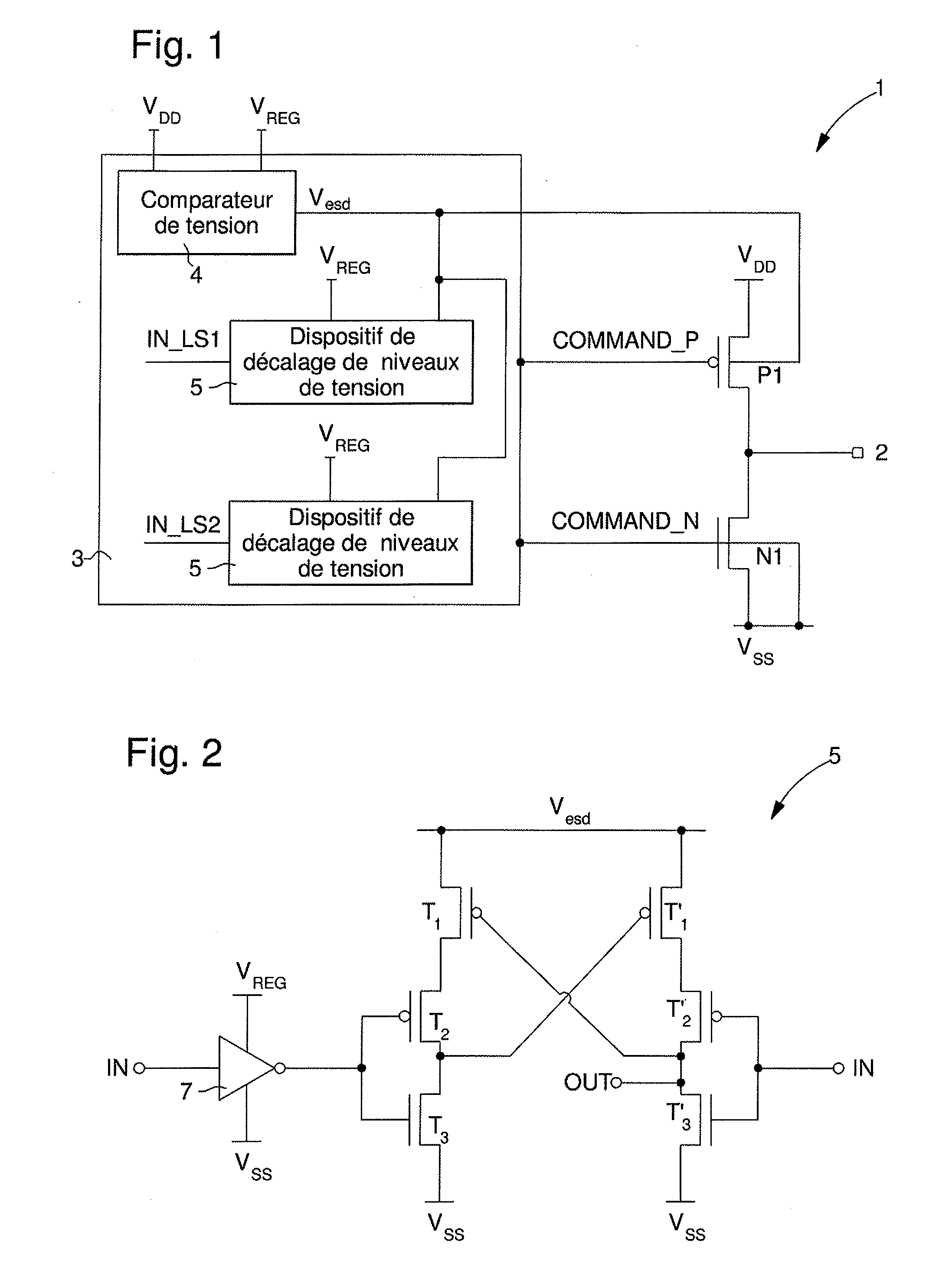
FIG. 1 shows schematically connection device 1 according to the present invention. This device 1 includes a buffer formed of two active transistors. The buffer includes more specifically one transistor P1 and one transistor N1 connected in series. Thus, the drains of the two transistors N1, P1 are connected to each other, whereas the source of transistor P1 is connected to supply voltage VDD and the source and well of transistor N1 is connected to earth VSS. The drains of both transistors are also connected to external contact pad 2 where an external component can be connected. The gates of these transistors N1, P1 are connected to the same potential, while the well of transistor P1 is biased at a voltage corresponding to the maximum amplitude value of the voltage signals controlling transistors ...


PUM


Abstract

The integrated circuit connection device (1) enables an external component to be connected. The integrated circuit is powered by a supply voltage (VDD) and part of the circuit operates using at least one internal regulated voltage (VREG). The connection device includes two active transistors (N1, P1) of different conductivity connected in series between the supply voltage (VDD) and earth (VSS). The drains of these two active transistors (N1, P1) are connected to each other so as to form an external contact pad (2). The gates of these active transistors are controlled by voltage signals that have the same amplitude (Vesd). The connection device further includes switching means (3) for modifying the control signals (Vesd) applied across the active transistor gates, without exceeding the highest voltage between the supply voltage (VDD) and the internal regulated voltage (VREG). This allows the voltage range of said integrated circuit to be adapted to an external component connected to the external contact pad (2).

Description

The invention concerns an integrated circuit connection device for connecting an external component. The integrated circuit is powered by a supply voltage and one part of the circuit operates using at least one internal regulated voltage. The connection device includes two active transistors of different conductivity series-connected between the supply voltage and earth. The drains of these two active transistors are connected to each other so as to form an external contact pad, and the gates of the active transistors are controlled by voltage signals having the same amplitude.BACKGROUND OF THE INVENTIONIntegrated circuit connection devices are known in the prior art. Indeed, integrated circuits are generally fitted with connection devices enabling the connection of external components and communication between the external element and said integrated circuit.These connection devices consist of two active MOS (PMOS and NMOS) transistors in an inverter arrangement to form a buffer. T...

Claims


Application Information

Patent Timeline
IPC IPC(8): H03L5/00
CPCH03K19/0027H03K19/018521H03K19/00315
Inventor THEODULOZ, YVESJAEGGI, HUGOPLAVEC, LUBOMIR
Owner EM MICROELECTRONIC-MARIN
Why Eureka
Try Eureka