Liquid crystal display panel and manufacturing method thereof

a technology of liquid crystal display panel and manufacturing method, which is applied in the direction of static indicating device, non-linear optics, instruments, etc., can solve the problems of small viewing angle, small aperture ratio, difficult to discharge static electricity, etc., and achieves simplified manufacturing process, improved liquid crystal efficiency, and simple structure

Active Publication Date: 2011-07-14
SAMSUNG DISPLAY CO LTD
View PDF11 Cites 10 Cited by
  • Summary
  • Abstract
  • Description
  • Claims
  • Application Information

AI Technical Summary

Benefits of technology

[0030]According to an exemplary embodiment of the present invention, because the conductive layer is formed on the front surface of the first substrate to remove static electricity, static electricity of the liquid crystal display panel can be prevented with a simple structure.
[0031]According to an exemplary embodiment of the present invention, because a certain voltage is applied to the conductive layer formed on the front surface of the first substrate, liquid crystal molecules of the liquid crystal layer between the conductive layer and the pixel array can be prevented from being vertically aligned, thus improving liquid crystal efficiency.
[0032]In the method of forming a liquid crystal display panel according to an exemplary embodiment of the present invention, because such a process of forming a conductive layer on a rear surface of the first substrate and grounding it from the exterior as in the related art is omitted, the manufacturing process of the liquid crystal display panel can be simplified and the productivity can be improved to lead to a reduction in production cost.

Problems solved by technology

The TN mode LCD, in which liquid crystal molecules of a liquid crystal display panel are driven by a vertical field formed between pixel electrodes and a common electrode disposed to face each other on an upper substrate, advantageously has a large aperture ratio but disadvantageously has a small viewing angle.
The IPS mode LCD, in which liquid crystal molecules of a liquid crystal display panel are driven by a horizontal field between pixel electrodes and a common electrode disposed in parallel to each other on a lower substrate, advantageously has a large viewing angle but disadvantageously has a small aperture ratio.
In comparison, in the IPS mode LCD, because the liquid crystal molecules of the liquid crystal display panel are driven by a horizontal field, the color filter array substrate is electrically isolated, making it difficult to discharge static electricity.
However, in the related art LCD, because the transparent metal layer is formed at the outer side of the liquid crystal display panel, a problem arises in that an etching process for making the liquid crystal display panel thinner cannot be performed.
In this case, however, when forming the transparent metal layer at the outer side of the liquid crystal display panel, the process of making the liquid crystal display panel thinner, which includes a dipping process with an etching solution, cannot be performed.

Method used


Image

  • Liquid crystal display panel and manufacturing method thereof
  • Liquid crystal display panel and manufacturing method thereof
  • Liquid crystal display panel and manufacturing method thereof

Examples


Embodiment Construction

[0037]The present invention will be described more fully hereinafter with reference to the accompanying drawings, in which exemplary embodiments of the invention are shown. In describing the present invention, a configuration required for understanding the technical ideas of the present invention will be mainly described, and a description of a configuration departing from the ideas of the present invention will be omitted. However, a skilled person in the art to which the present invention pertains will understand the technical scope of the ideas of the present invention. As those skilled in the art would realize, the described embodiments may be modified in various different ways, all without departing from the spirit or scope of the present invention. The drawings and description are to be regarded as illustrative in nature and not restrictive. Like reference numerals designate like elements throughout the specification.

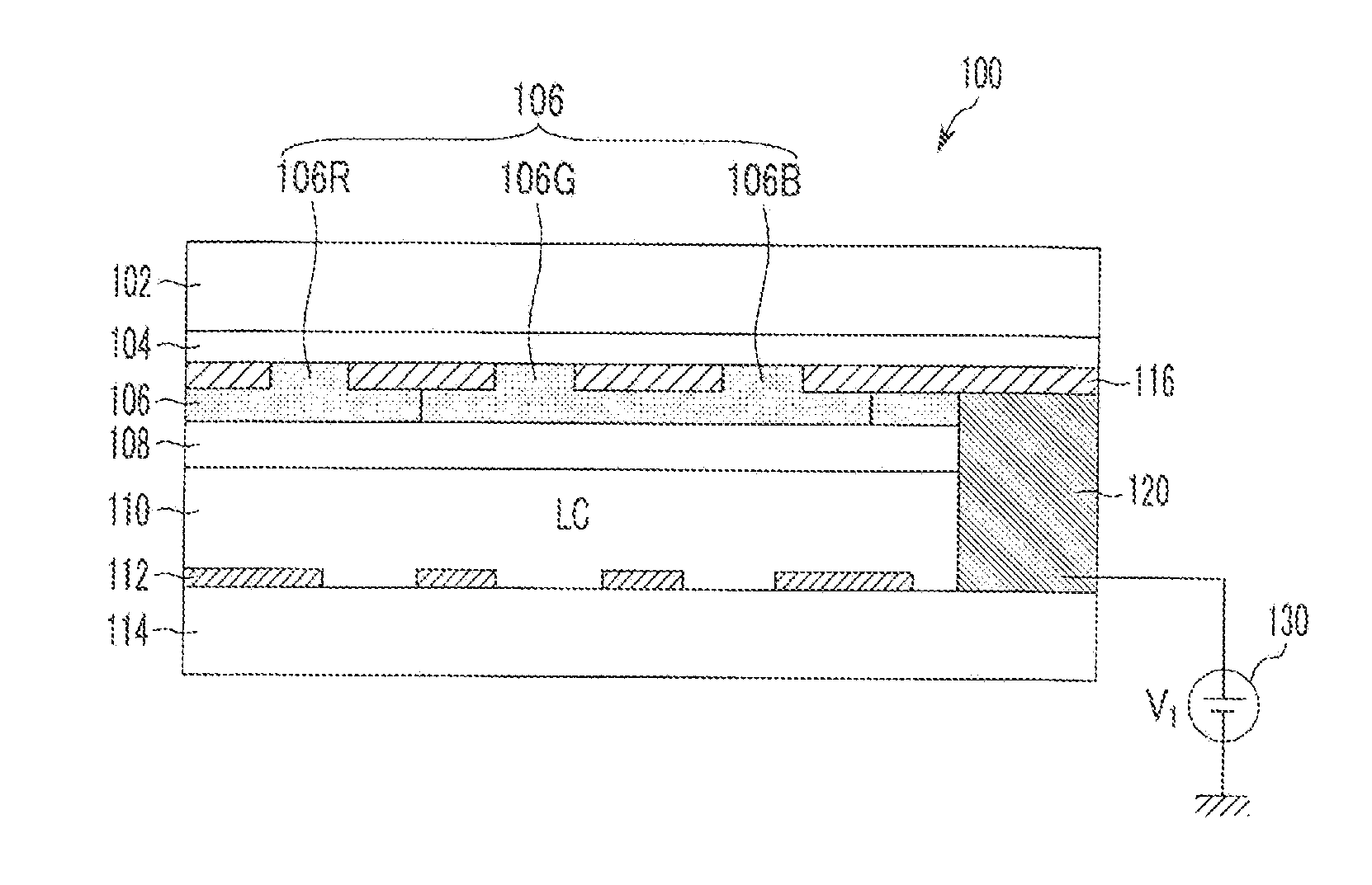
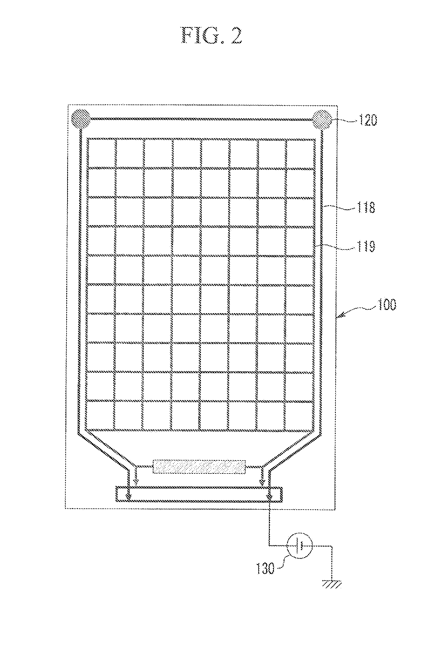
[0038]FIG. 1 is a cross-sectional view of a liquid crystal d...


PUM

PropertyMeasurementUnit
reference voltageaaaaaaaaaa
voltageaaaaaaaaaa
voltageaaaaaaaaaa

Abstract

A liquid crystal display panel is disclosed. The liquid crystal display panel includes: a first substrate with a conductive layer formed on one surface thereof; a color filter layer including a plurality of color filters formed on the conductive layer; a conductive light shielding layer formed between the plurality of color filters; a second substrate with a pixel array formed on one surface thereof; and a liquid crystal layer filled between the conductive light shielding layer and the pixel array, wherein the conductive layer is electrically short-circuited with the pixel array. Since a voltage is applied to the conductive layer formed on the front surface of the first substrate, liquid crystal molecules of the liquid crystal layer between the conductive layer and the pixel array can be prevented from being vertically aligned, thus improving liquid crystal efficiency.

Description

CLAIM OF PRIORITY[0001]This application claims priority to and the benefit of Korean Patent Application No. 10-2010-0001979 filed in the Korean Intellectual Property Office on Jan. 8, 2010, the entire contents of which are incorporated herein by reference.BACKGROUND OF THE INVENTION[0002]1. Field of the Invention[0003]The present invention relates to a liquid crystal display panel and manufacturing method thereof, and more particularly, to a liquid crystal display panel that is capable of preventing a vertical field due to static electricity with a simple configuration by positioning ITO within a color filter and applying an internal voltage and a threshold voltage, and a manufacturing method thereof.[0004]2. Description of the Related Art[0005]In general, a liquid crystal display (LCD) displays an image corresponding to a video signal on a liquid crystal display panel, on which liquid crystal cells are arranged in a matrix form, by adjusting light transmittance of the liquid crysta...

Claims


Application Information

Patent Timeline
Patent Type & Authority Applications(United States)
IPC IPC(8): G02F1/133G02F1/1333
CPCG02F1/13452G02F1/133512
Inventor LIM, DONG-HUNKIM, MIN-WOO
Owner SAMSUNG DISPLAY CO LTD
Why Eureka
Try Eureka