Semiconductor device

a technology of semiconductors and semiconductors, applied in the direction of semiconductor devices, electrical devices, transistors, etc., can solve the problems of high manufacturing cost per substrate unit area, microcrystalline silicon tfts have not yet been commercialized, etc., and achieve the effect of reducing the off current of tfts

Active Publication Date: 2011-06-23
SHARP KK
View PDF3 Cites 20 Cited by
  • Summary
  • Abstract
  • Description
  • Claims
  • Application Information

AI Technical Summary

Benefits of technology

[0033]The present invention provides a semiconductor device capable of offering OFF currents that are lower than in the conventional art. While the present invention is particularly effective for reducing the OFF currents of TFTs having an active layer including a microcrystalline silicon film, the prevent invention can reduce the OFF currents of TFTs regardless of type of semiconductor film.

Problems solved by technology

Manufacturing of the polysilicon TFTs, however, requires complicated steps, including a laser crystallization step for crystallizing an amorphous silicon film, a thermal anneal step, and an ion doping step, which contribute to higher manufacturing cost per substrate unit area.
In spite of offering many advantages described above, microcrystalline silicon TFTs have yet to be commercialized to date.

Method used


Image

  • Semiconductor device
  • Semiconductor device
  • Semiconductor device

Examples


Embodiment Construction

[0043]Preferred embodiments of semiconductor devices of the present invention are described with reference to the drawings. While examples of TFTs having a microcrystalline silicon film as an active layer are described, the present invention is not limited to such examples.

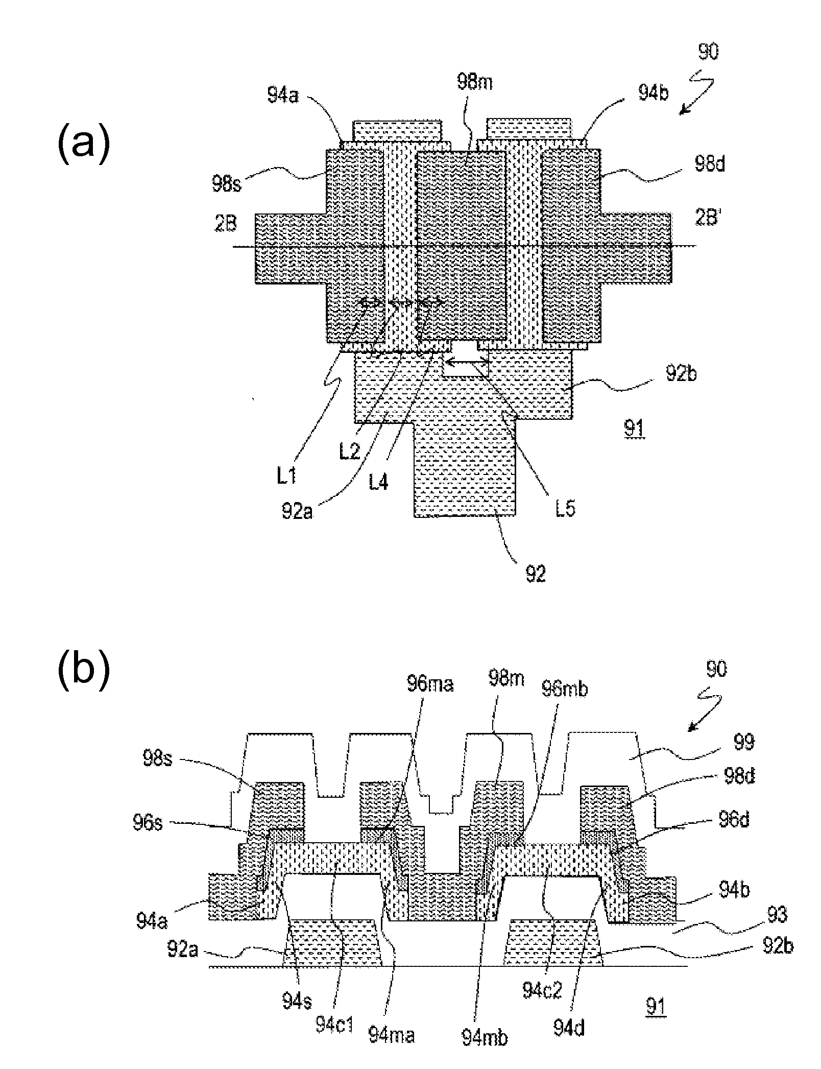
[0044]FIG. 1 shows a schematic of TFT 10 according to a preferred embodiment of the present invention. FIG. 1(a) is a schematic plan view of TFT 10; FIG. 1(b) is a cross-sectional schematic along the line 1B-1B′ in FIG. 1(a); and FIG. 1(c) shows an equivalent circuit diagram for TFT 10.

[0045]TFT 10 has a dual gate structure and is electrically equivalent to a structure having two TFTs that are connected in series, as shown in the equivalent circuit diagram in FIG. 1(c).

[0046]TFT 10 includes an active layer 14, which is supported by a substrate 11 (for example, a glass substrate). Active layer 14 is a semiconductor layer and includes a microcrystalline silicon film. Active layer 14 includes channel regions 14c1 and...


PUM


Abstract

A semiconductor device 10 according to the present invention includes an active layer 14 supported on a substrate 11 and having two channel regions 14c1, 14c2, a source region 14s, a drain region 14d, and an intermediate region 14m formed between the two channel regions 14c1, 14c2; a contact layer 16 having a source contact region 16s, a drain contact region 16d, and an intermediate contact region 16m; a source electrode 18s; a drain electrode 18d; an intermediate electrode 18m; and a gate electrode 12 facing the two channel regions and the intermediate region through a gate insulating film 13 interposed therebetween. An entire portion of the intermediate electrode 18m that is located between the first channel region 14c1 and the second channel region 14c2 overlaps the gate electrode 12 through the intermediate region 14m and the gate insulating film 13.

Description

TECHNICAL FIELD[0001]The present invention relates to a semiconductor device, and in particular, to a semiconductor devices having a semiconductor layer supported on a substrate.BACKGROUND ART[0002]Liquid crystal display devices and organic EL display devices, which include a thin film transistor (TFT) for each pixel, have been in wide use in recent years. TFTs are manufactured using a semiconductor layer formed on a substrate, such as a glass substrate. A substrate on which the TFTs have been formed is called an active matrix substrate.[0003]As such TFTs, TFTs with an amorphous silicon film as the active layer (amorphous silicon TFTs) and TFTs with a polysilicon film as the active layer (polysilicon TFTs) have been widely used.[0004]Because the carrier mobility in a polysilicon film is higher than in an amorphous silicon film, polysilicon TFTs offer higher ON currents and operate faster than amorphous silicon TFTs. For this reason, display panels having polysilicon TFTs not only fo...

Claims


Application Information

Patent Timeline
Patent Type & Authority Applications(United States)
IPC IPC(8): H01L29/786
CPCH01L27/3262H01L29/78609H01L29/41733H01L29/78696H01L29/78645H10K59/1213
Inventor MORIGUCHI, MASAOYOSHIDA, TOKUOSAITOH, YUHICHIIWASE, YASUAKIKANZAKI, YOSUKESAKAMOTO, MAYUKO
Owner SHARP KK
Why Eureka
Try Eureka