
Touch-sensing structure for touch panel and touch-sensing method thereof

Active Publication Date: 2011-03-10
AU OPTRONICS CORP
View PDF6 Cites 6 Cited by
  • Summary
  • Abstract
  • Description
  • Claims
  • Application Information

AI Technical Summary

Benefits of technology

[0013]The present invention relates to a touch-sensing structure for a touch panel. A touch screen using the touch-sensing structure can attain high sensing resolution without employing a touch signal processing circuit having a great number of channels. Moreover, peripheral wires for the touch panel of the touch screen can be reduced, and thereby it is unnecessary to enlarge the width of the edge portion for the touch panel. Further, compared with the conventional passive touch-sensing structure, the touch-sensing structure provided in the present invention has an ability of performing multi touch sensing. In addition, compared with the conventional active touch-sensing structure, the aperture ratio of the pixel in the touch-sensing structure provided in the present invention would not be reduced, and the touch-sensing response time thereof can also be faster.
[0021]As described above, the present invention mainly utilizes the above conductor to obtain the coordinates of the touch position, and the touch signal processing circuit can carry out such operation merely through being coupled to the terminals of the conductor. Thus, the touch screen using the touch-sensing structure provided in the present invention can attain high sensing resolution without employing a touch signal processing circuit having a great number of channels. Moreover, peripheral wires for the touch panel of the touch screen can be less, and thereby it is unnecessary to enlarge the width of the edge portion for the touch panel. Further, as the resistances of the two equivalent resistors can respectively be measured at the two terminals of a same conductor, so as to represent different numbers of line segments, or to calculate the distance between the touch position and the terminals of the conductors according to the resistances of the two equivalent resistors, the touch-sensing structure provided in the present invention has an ability of performing multi touch sensing, while compared with the conventional passive touch-sensing structure. In addition, compared with the conventional active touch-sensing structure, it is not necessary to employ any transistor to form the sensing unit in the touch-sensing structure provided in the present invention, and accordingly the aperture ratio of the pixel in the touch panel can be ensured, and the touch-sensing response time thereof can also be lowered.

Problems solved by technology

This may increase the cost of the touch screen.
Furthermore, another deficiency arises in this kind of passive touch-sensing structure, specifically, the touch-sensing structure can only perform a so-called single touch sensing.
This may increase the cost of the touch screen.

Method used


Image

  • Touch-sensing structure for touch panel and touch-sensing method thereof
  • Touch-sensing structure for touch panel and touch-sensing method thereof
  • Touch-sensing structure for touch panel and touch-sensing method thereof

Examples


first embodiment

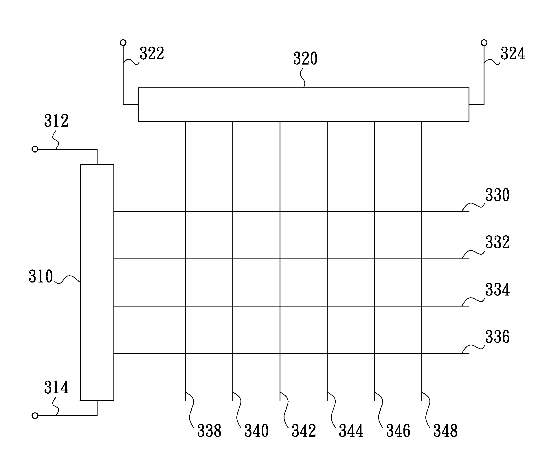
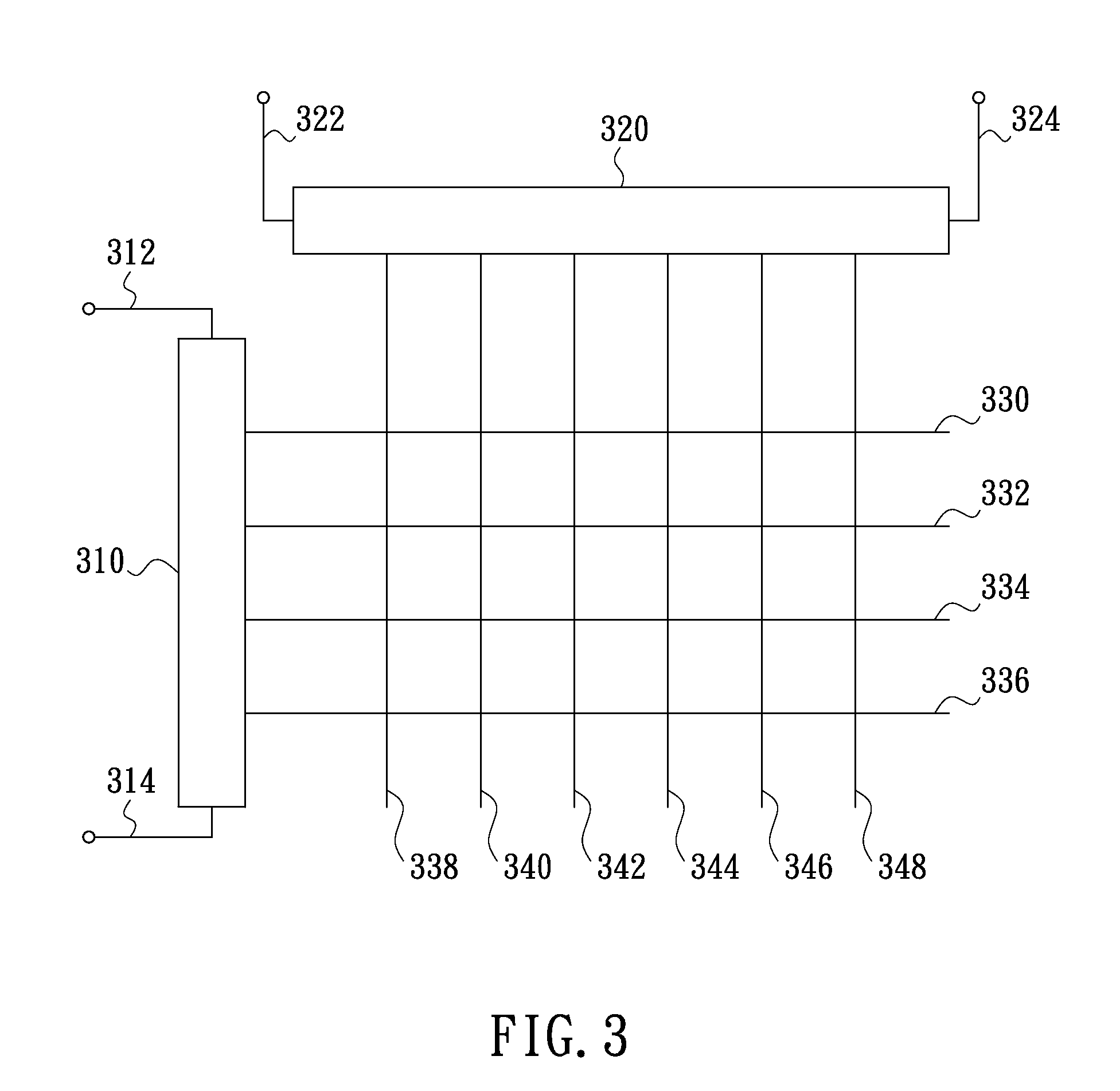
[0040]Referring to FIG. 3, a touch-sensing structure for a touch panel according to the present invention is illustrated. The touch-sensing structure is applicable for sensing two-dimension coordinates of a touch position. As FIG. 2 shown, the touch-sensing structure includes a first conductor 310, a second conductor 320, and a plurality of conducting wires 330-348. Moreover, the touch-sensing structure further includes touch-signal reading lines 312, 314, 322, and 324. The conducting wires 330-336 are disposed in parallel, and one terminal of each of the conducting wires 330-336 is electrically coupled to the first conductor 310, so as to divide the first conductor 310 into a plurality of first line segments. The conducting wires 338-348 are disposed in parallel and substantially perpendicular to the conducting wires 330-336. One terminal of each of the conducting wires 338-348 is electrically coupled to the second conductor 320, so as to divide the second conductor 320 into a plur...

eighth embodiment

[0066]Based on the teaching of the eighth embodiment, a basic operation method can be summarized as FIG. 15. FIG. 15 is a flow chart of a touch-sensing method according to another embodiment of the present invention, which can be applied in a touch panel. The touch panel has a touch-sensing structure, and the touch-sensing structure includes a first conductor and tow touch-signal reading lines. The conductor includes N parallel conducting structures, each of which includes a first terminal and a second terminal. The first terminal and the second terminal point to a first direction and a second direction, respectively. The first terminal of the first conducting wire of the Kth conducting structure is electrically coupled to the first terminal of the second conducting wire of the Kth conducting structure, and the second terminal of the second conducting wire of the Kth conducting structure is electrically coupled to the second terminal of the first conducting wire of the (K+1)th condu...


PUM


Abstract

In a touch-sensing structure for a touch panel and a touch-sensing method thereof, the touch-sensing structure includes a plurality of first conducting wires paralleled to each other and a first conductor. A terminal of each first conducting wire is electrically coupled to the first conductor, so as to divide the conductor into a plurality of first line segments. The resistance of each first conducting wire is smaller than that of each first line segment. Wherein, when the displaying area of the touch panel receives an external force, a first conducting wire corresponding to the position designated by the external force is electrically coupled to a reference potential.

Description

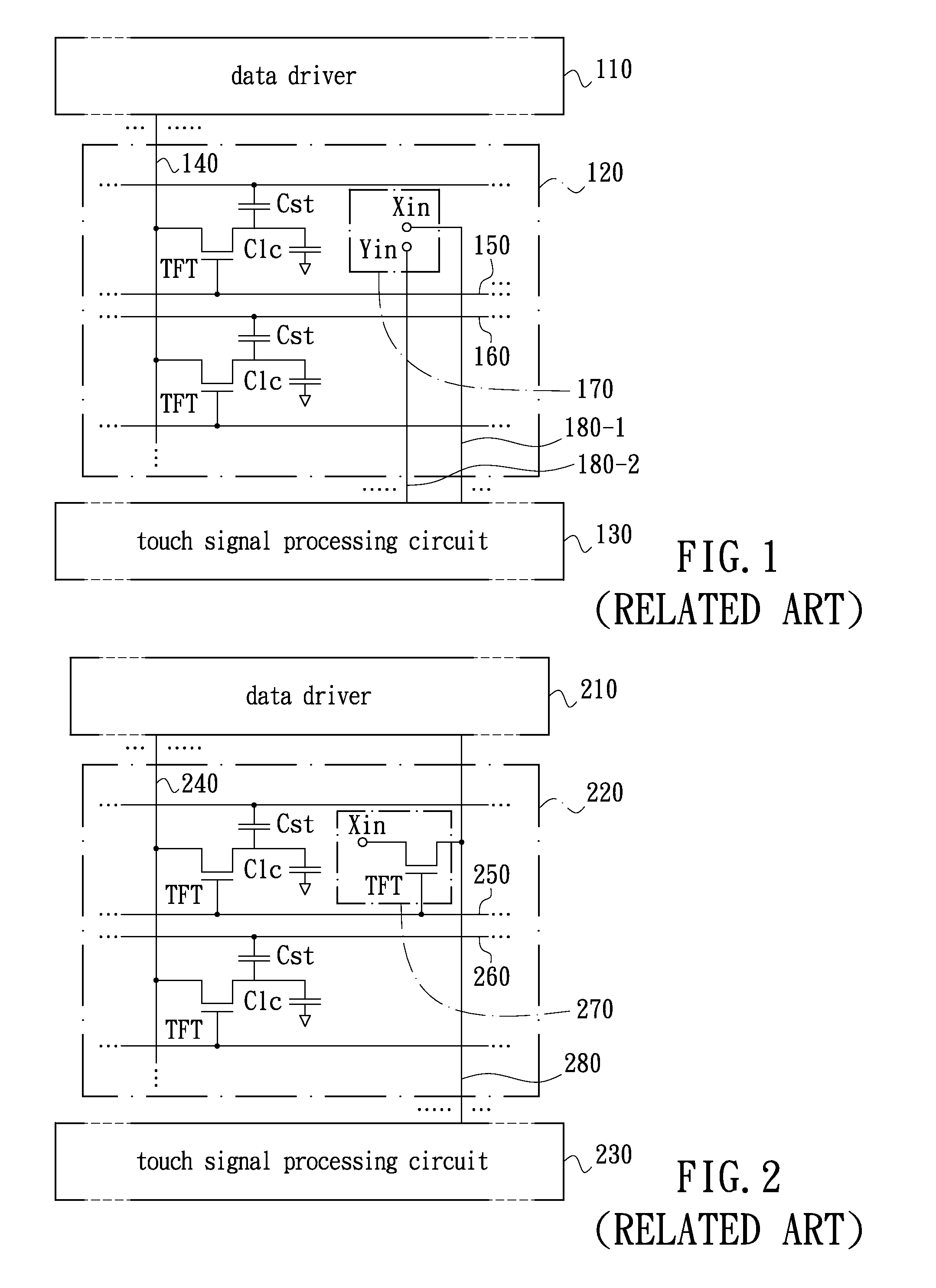
CROSS-REFERENCE TO RELATED APPLICATIONS[0001]This application is based upon and claims the benefit of priority from the prior Taiwan Patent Application No. 098130297, filed Sep. 8, 2009, the entire contents of which are incorporated herein by reference.BACKGROUND[0002]1. Technical Field[0003]The present invention relates to a touch panel, and more particularly, to a touch-sensing structure for a touch panel, and a touch-sensing method thereof.[0004]2. Description of the Related Art[0005]With development of the touch screen, nowadays, two kinds of touch-sensing structures for embedded touch screen are used widely, one of which is a passive touch-sensing structure, and the other one is an active touch-sensing structure. The two kinds of touch-sensing structures are respectively shown in FIG. 1 and FIG. 2.[0006]FIG. 1 is a schematic view of a touch screen employing the passive touch-sensing structure. Referring to FIG. 1, the touch screen includes a data driver 110, a touch panel 120, ...

Claims


Application Information

Patent Timeline
IPC IPC(8): G06F3/041
CPCG06F2203/04104G06F3/047
Inventor HUANG, KUNG-CHIEHHUANG, HONG-JILEE, SEOK-LYUL
Owner AU OPTRONICS CORP
Learn More