
Low noise signal reproducing method for a solid state imaging device

a solid-state imaging and low-noise signal technology, applied in the direction of color television details, television system details, television systems, etc., can solve the problem that the image in which the pixel mixture readout method can be applied is limited to relatively dark scenes, and achieves the effect of reducing not only the reset noise, avoiding the saturation of the voltage conversion part, and low-noise signal

Inactive Publication Date: 2011-03-03
OZAWA NAOKI
View PDF8 Cites 1 Cited by
  • Summary
  • Abstract
  • Description
  • Claims
  • Application Information

AI Technical Summary

Benefits of technology

"The present invention provides a method for reducing noise in a solid state imaging device by controlling the reset pulse based on the output signal of the device. This method prevents saturation of the voltage conversion part in bright scenes and reduces amplifier noise around frequency zero, resulting in improved signal quality. Additionally, this method allows for the reproduction of many pixel signals as a differential signal, further reducing amplifier noise."

Problems solved by technology

So, though the prior method employing the pixel mixture readout operation can reduce not only the reset noise but the amplifier noise around frequency zero, an image in which the pixel mixture readout method can be applied is limited to relatively dark scene.

Method used


Image

  • Low noise signal reproducing method for a solid state imaging device
  • Low noise signal reproducing method for a solid state imaging device
  • Low noise signal reproducing method for a solid state imaging device

Examples


Embodiment Construction

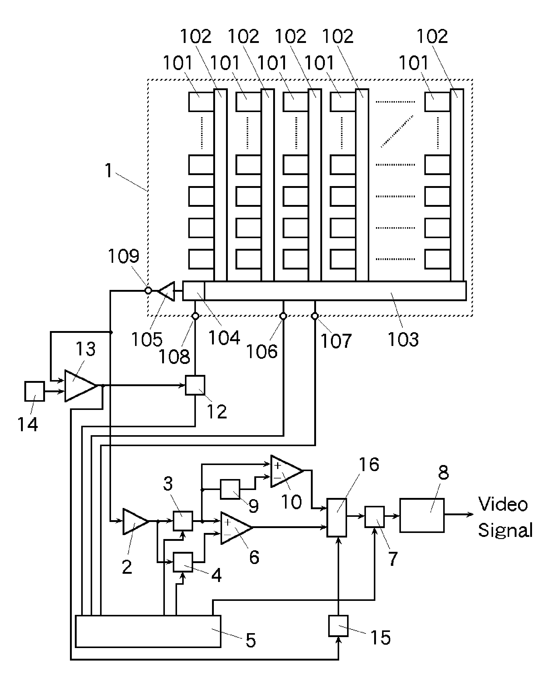
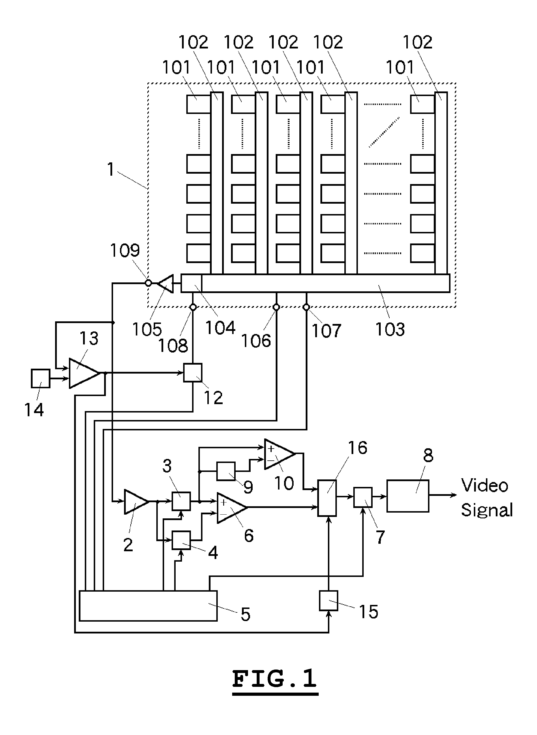
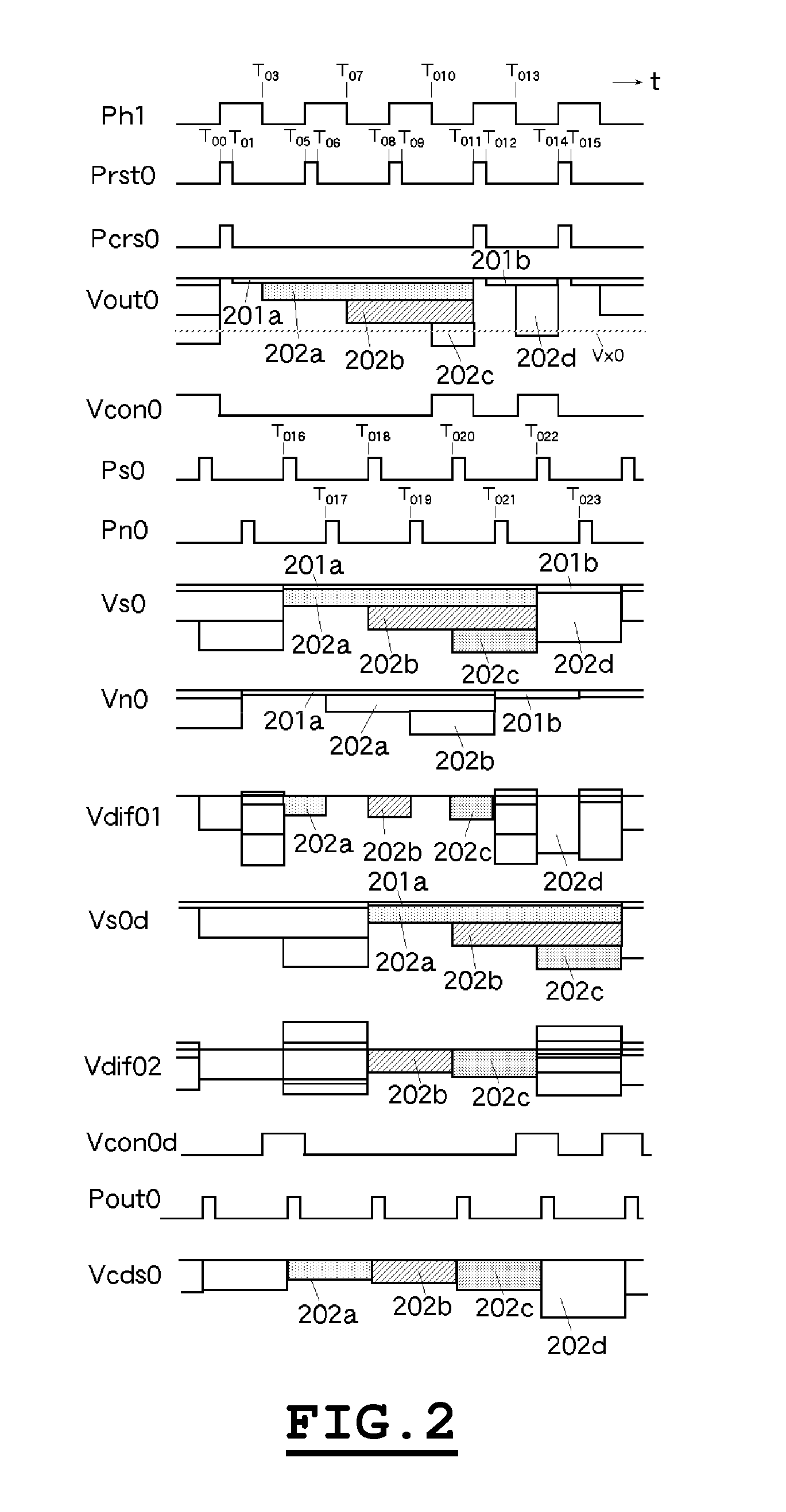
[0057]Referring now to the drawings, exemplary embodiments of the invention will be described. An example of the imaging apparatus in which the invention is applied is shown in FIG. 1. And, the timing diagram concerning to the signal reproducing method of the invention is shown in FIG. 2.

[0058]In the imaging apparatus shown in FIG. 1, reference numeral 1 represents a CCD imaging device. The basic operation of the CCD imaging device 1 in FIG. 1 is same as that of the prior art shown in FIG. 6. Namely, the signal charges generated during the fixed exposure period and accumulated to each pixel 101 are read to corresponding vertical CCD 102 at every vertical blanking period simultaneously by operation of transfer gates which are not shown in a figure. And, the signal charges read to each vertical CCD 102 are transferred toward a horizontal CCD 103 by one step at every horizontal blanking period. Moreover, the signal charges transferred to the horizontal CCD 103 are transferred toward a ...


PUM


Abstract

A method for reproducing a low noise signal for a solid state imaging device which can reduce not only the reset noise but the amplifier noise around frequency zero, avoiding the saturation of the voltage conversion part in a bright scene, is accomplished by controlling a reset pulse of a CCD imaging device according to the result of comparing the output signal of the CCD imaging device with a reference signal value. When the output signal of the CCD imaging device is smaller than the reference signal value, the reset pulse is not applied to the CCD imaging device. Thereat, a pixel signal is reproduced as a differential signal between two signals sampled at two points with an interval of T0, the amplifier noise around frequency zero being reduced in the pixel signals.

Description

CROSS-REFERENCE TO RELATED APPLICATION[0001]Not ApplicableBACKGROUND OF THE INVENTION[0002]1. Field of the Invention[0003]This invention relates to solid state imaging device technology, and more particularly, to such signal reproducing methods for providing low noise output signals from a solid state imaging device.[0004]2. Description of the Prior Art[0005]A solid state imaging device is employed in numerous image capturing apparatuses including digital still cameras. In a solid state imaging device for digital still cameras, the size of a pixel is miniaturized with the increase in the number of pixels on an imaging device more and more. Since miniaturization of pixel size causes reduction of the signal level from a pixel, reduction of the noise on the signal is important to keep the signal to noise ratio of a reproduced picture high.[0006]The noise generated in a CCD imaging device, being a main kind of the solid state imaging device, comprises shot noise correlated to the signal...

Claims


Application Information

Patent Timeline
Patent Type & Authority Applications(United States)
IPC IPC(8): H04N5/335H04N25/00
CPCH04N5/3722H04N25/715
Inventor OZAWA, NAOKI
Owner OZAWA NAOKI
Learn More