
MOSFET device with reduced breakdown voltage

a technology of mosfet and breakdown voltage, which is applied in the direction of semiconductor devices, diodes, electrical apparatus, etc., can solve the problems of gate oxide thickness reduction, more pronounced problems, and more easily damaged gate oxide during operation

Active Publication Date: 2011-02-24
ALPHA & OMEGA SEMICON INC
View PDF5 Cites 37 Cited by
  • Summary
  • Abstract
  • Description
  • Claims
  • Application Information

AI Technical Summary

Benefits of technology

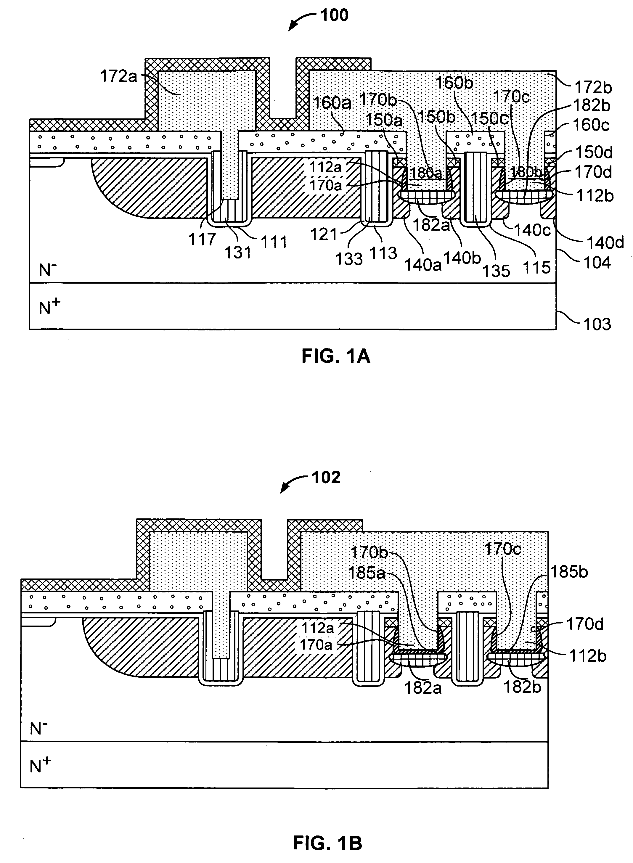
[0019]The embodiments shown above use N-type substrate (i.e., an N+ silicon wafer with an N− epi layer grown on the wafer) as the drain of the device. In some embodiments, P-type substrate is used and the devices have N-type body contact implants and P-type epi enhancement layers.

Problems solved by technology

As device size decreases, the thickness of gate oxide within the device also decreases and becomes more easily damaged during operation.
The problem is more pronounced in power MOSFET devices, which often conduct high current and dissipate a large amount of power.

Method used


Image

  • MOSFET device with reduced breakdown voltage
  • MOSFET device with reduced breakdown voltage
  • MOSFET device with reduced breakdown voltage

Examples


Embodiment Construction

[0007]The invention can be implemented in numerous ways, including as a process; an apparatus; a system; a composition of matter; a computer program product embodied on a computer readable storage medium; and / or a processor, such as a processor configured to execute instructions stored on and / or provided by a memory coupled to the processor. In this specification, these implementations, or any other form that the invention may take, may be referred to as techniques. In general, the order of the steps of disclosed processes may be altered within the scope of the invention. Unless stated otherwise, a component such as a processor or a memory described as being configured to perform a task may be implemented as a general component that is temporarily configured to perform the task at a given time or a specific component that is manufactured to perform the task. As used herein, the term ‘processor’ refers to one or more devices, circuits, and / or processing cores configured to process da...


PUM


Abstract

A semiconductor device includes a drain, an epitaxial layer overlaying the drain, and an active region. The active region includes a body disposed in the epitaxial layer, a source embedded in the body, a gate trench extending into the epitaxial layer, a gate disposed in the gate trench, a contact trench extending through the source and at least part of the body, a contact electrode disposed in the contact trench, and an epitaxial enhancement portion disposed below the contact trench, wherein the epitaxial enhancement portion has the same carrier type as the epitaxial layer.

Description

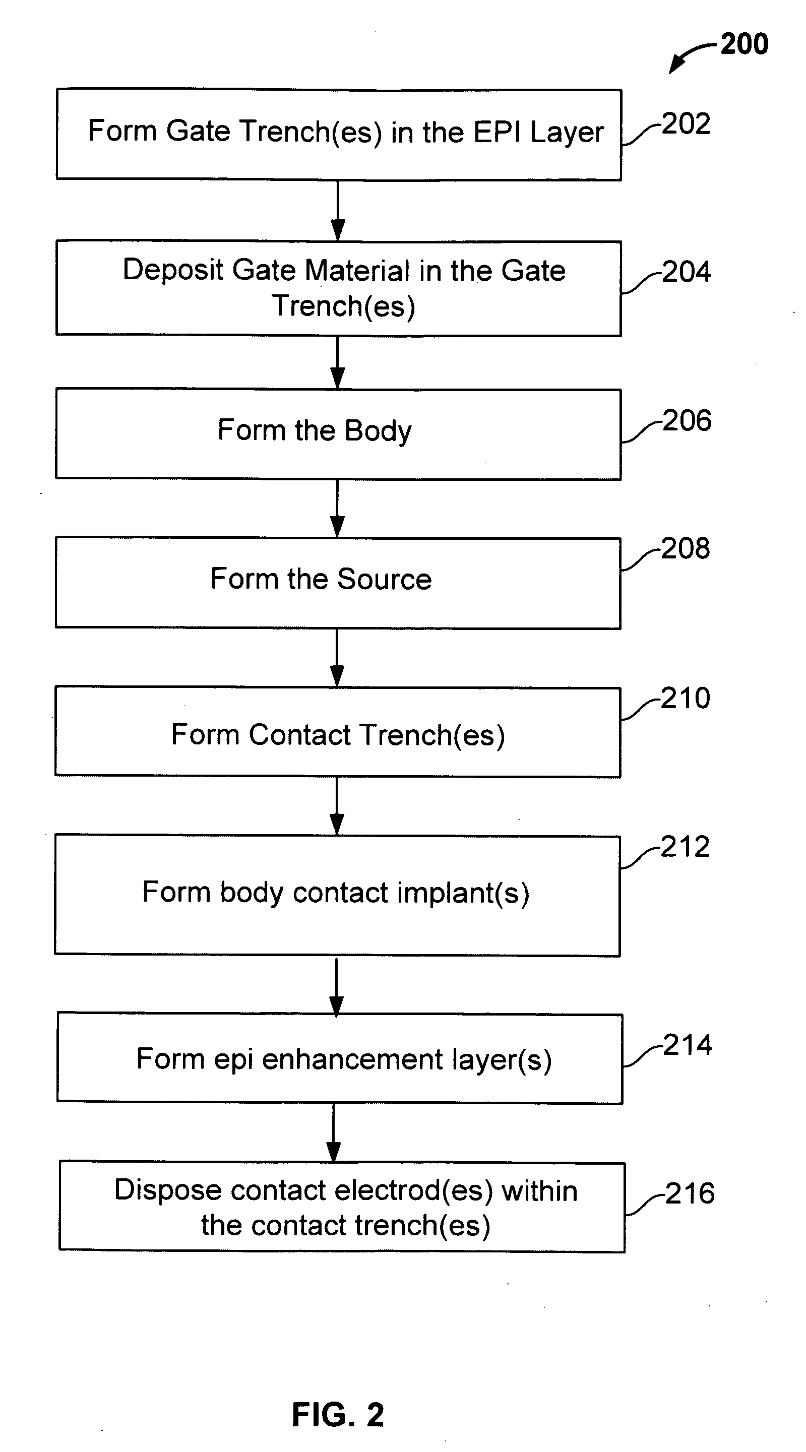
BACKGROUND OF THE INVENTION[0001]Modern semiconductor devices, such as Metal Oxide Semiconductor Field Effect Transistors (MOSFETs) are often high density devices with small feature sizes. For example, the wall-to-wall pitch size of some MOSFETs in use today is on the order of 1-2 μms. As device size decreases, the thickness of gate oxide within the device also decreases and becomes more easily damaged during operation. The problem is more pronounced in power MOSFET devices, which often conduct high current and dissipate a large amount of power.BRIEF DESCRIPTION OF THE DRAWINGS[0002]Various embodiments of the invention are disclosed in the following detailed description and the accompanying drawings.[0003]FIGS. 1A-1B are cross-sectional diagrams illustrating embodiments of double-diffused metal oxide semiconductor (DMOS) devices with reduced breakdown voltage.[0004]FIG. 2 is a flowchart illustrating an embodiment of a fabrication process for constructing a DMOS device.[0005]FIGS. 3A...

Claims


Application Information

Patent Timeline
IPC IPC(8): H01L29/47H01L21/28
CPCH01L21/26586H01L29/1037H01L29/1095H01L29/41766H01L29/4236H01L29/47H01L29/66128H01L29/66143H01L29/66727H01L29/66734H01L29/7806H01L29/7811H01L29/7813H01L29/8611H01L29/872H01L29/7827H01L29/8725H01L21/26513H01L29/0878H01L29/0865H01L21/30604H01L29/7804H01L29/7808
Inventor PAN, JIBHALLA, ANUP
Owner ALPHA & OMEGA SEMICON INC
Learn More