Modular prototyping of a circuit for manufacturing

a technology of electronic circuit board and manufacturing process, applied in the direction of printed circuit aspects, stacked spaced pcbs, stacked pcbs, etc., can solve the problems of high cost of manufacturing a single or small quantity of electronic circuit boards, time-consuming and laborious construction of prototypes, and prone to errors. , to achieve the effect of reducing the cost of manufacturing

Inactive Publication Date: 2011-02-03
CASKA JAMES PETER
View PDF1 Cites 7 Cited by
  • Summary
  • Abstract
  • Description
  • Claims
  • Application Information

AI Technical Summary

Problems solved by technology

However, the cost for manufacturing a single or small quantity of electronic circuit boards can be very high due to the lack of amortization of the relatively high set up costs.
For all their benefits, prototypes can be time consuming to build and prone to errors during construction due to the nature of the wiring and can require considerable skill and mechanical and electrical aptitude to construct.
Another issue is that a prototype

Method used


Image

  • Modular prototyping of a circuit for manufacturing
  • Modular prototyping of a circuit for manufacturing
  • Modular prototyping of a circuit for manufacturing

Examples


Embodiment Construction

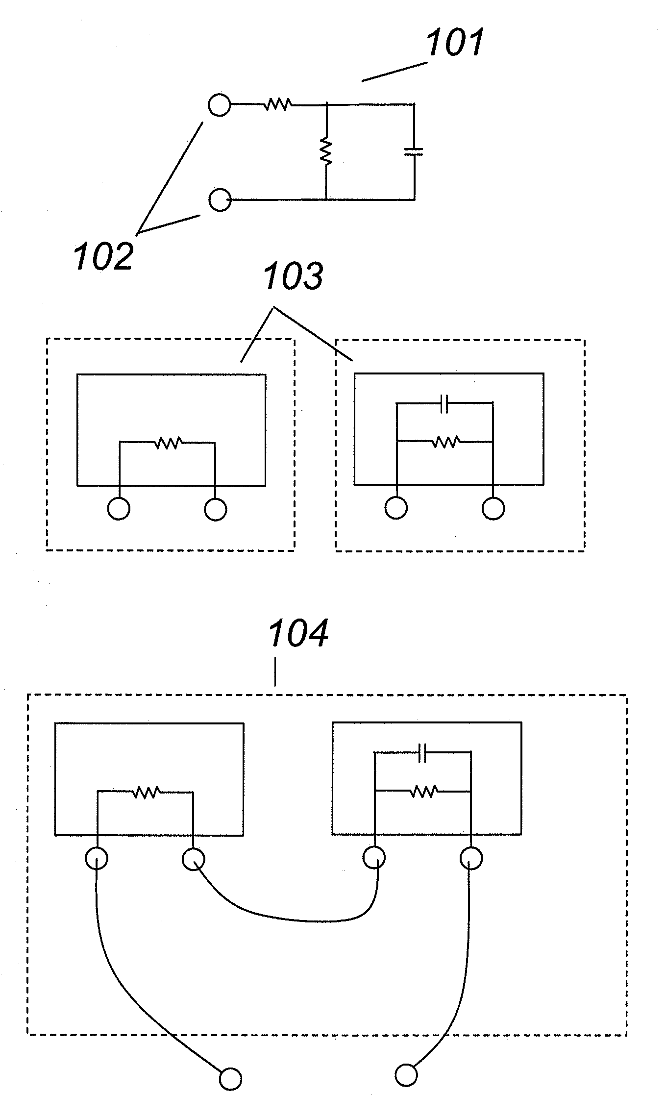
[0034]Various embodiments of the present invention will be described in detail with reference to the drawings, where like reference numerals represent like parts and assemblies throughout the several views. Reference to various embodiments does not limit the scope of the invention, which is limited only by the scope of the claims attached hereto. Additionally, any examples set forth in this specification are not intended to be limiting and merely set forth some of the many possible embodiments for the claimed invention.

[0035]Throughout the specification and claims, the following terms take at least the meanings explicitly associated herein, unless the context dictates otherwise. The meanings identified below do not necessarily limit the terms, but merely provide illustrative examples for the terms. The meaning of “a,”“an,” and “the” includes plural reference, and the meaning of “in” includes “in” and “on.” The phrase “in one embodiment,” as used herein does not necessarily refer to ...


PUM

PropertyMeasurementUnit
Densityaaaaaaaaaa

Abstract

An integrated method of prototyping and manufacturing electronic circuit boards where a new circuit design can move between virtual, prototype, partially merged and fully merged forms in a relatively automated fashion. A scaleable high density matrix of solderless electrical connections between the pin-outs of a plurality of electronic modules forms a virtual breadboard prototype circuit that can be merged into printed circuit board electrical layers to thus directly synthesize manufacturable forms of prototyped electronic circuits.

Description

CROSS REFERENCE TO RELATED APPLICATION[0001]This application claims the benefit of U.S. Provisional Application, titled “MODULAR MANUFACTURABLE BREADBOARD SYSTEM, ” Ser. No. 61 / 230,563 filed on Jul. 31, 2009, the benefit of which is hereby claimed under 35 U.S.C. §119(e), and which is further incorporated herein by reference.FIELD OF THE INVENTION[0002]The invention is directed to the design of electronic circuit boards, and more specifically to enabling the arrangement and testing of a variety of different electronic circuits prior to their manufacture on a printed circuit board.BACKGROUND OF THE INVENTION[0003]Printed circuit boards are commonly used to provide electronic circuits for a wide variety of applications. In the manufacturing process, conductive traces are deposited on the substrate of the circuit board and discrete electronic components are assembled thereon. In large quantities the cost of manufacturing an electronic circuit board can be relatively inexpensive because...

Claims


Application Information

Patent Timeline
IPC IPC(8): B23P19/00
CPCH05K1/0287H05K1/0289H05K1/142H05K1/144Y10T29/53174H05K2201/042H05K2201/10189H05K2201/10303H05K2201/041
Inventor CASKA, JAMES PETER
Owner CASKA JAMES PETER
Why Eureka
Try Eureka