Molding method, optical element manufacturing method, and arrayed optical element
a manufacturing method and optical element technology, applied in the field of molding methods of optical elements, can solve the problems of difficult to expect a shape-transferability with high accuracy, inability to manufacture large number of individual optical elements, and high pressure on inorganic materials from one direction, so as to reduce work burden, facilitate assembly, and reduce the effect of labor intensity
- Summary
- Abstract
- Description
- Claims
- Application Information
AI Technical Summary
Benefits of technology
Problems solved by technology
Method used
Image

Examples
first embodiment
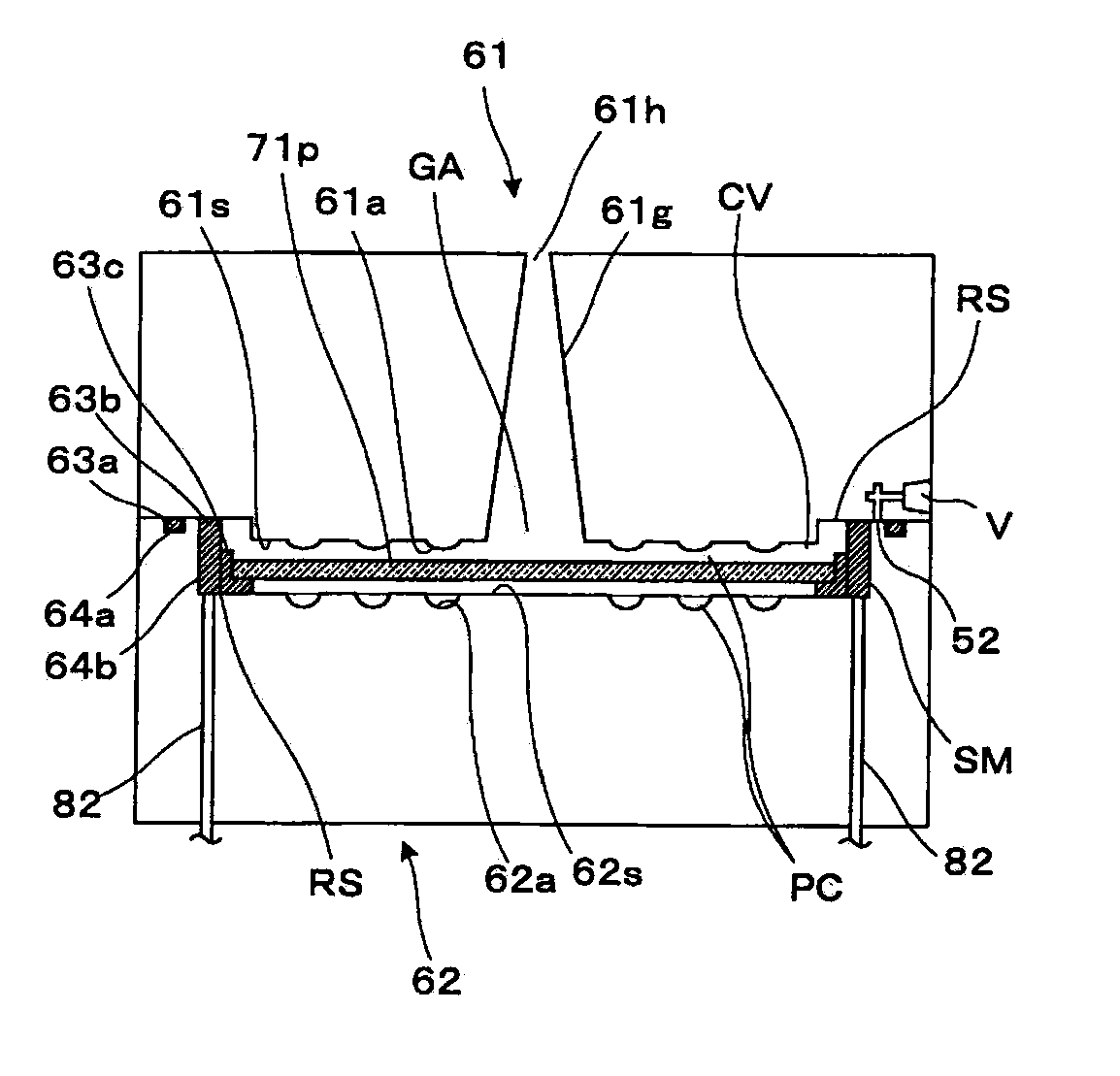
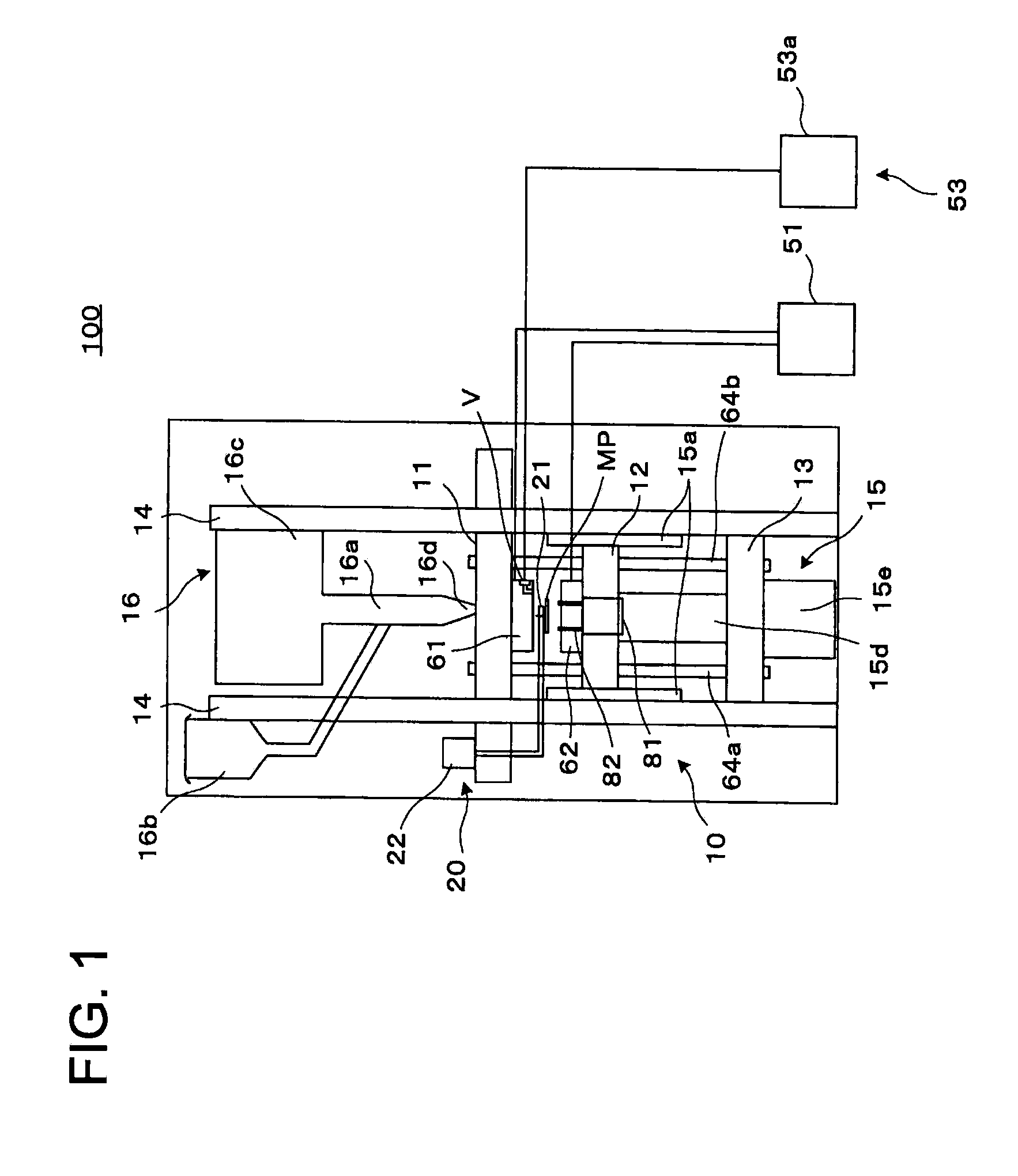
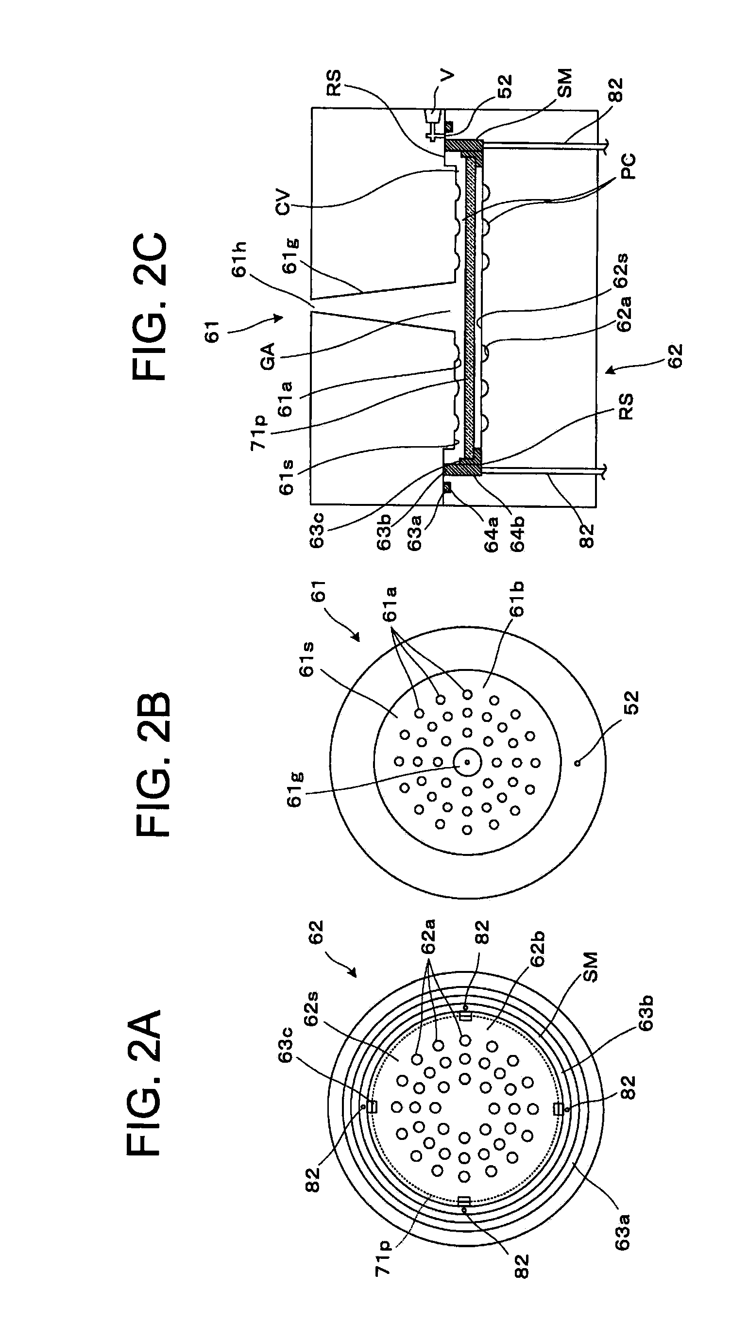
[0044]The molding method and optical element manufacturing method of the first embodiment of the present invention will be described referring to the drawings. FIG. 1 is a front view which conceptually illustrates the structure of an injection-molding apparatus for carrying out the molding method of the present embodiment.
[0045]Injection molding apparatus 100 of the present embodiment is provided with injection molding machine 10, transfer unit 20, temperature control unit 51, and decompression unit 53. Injection molding machine 10 is a part which performs injection molding to form molded body MP. Transfer unit 20 is a part which sets the optical plate, which will be mentioned later, in injection molding machine 10 and which takes out molded body MP from injection molding machine 10. Temperature control unit 51 is a part which adjusts the temperature of molds 61 and 62 of injection molding machine 10. Decompression unit 53 is a part which carries out vacuum suction of the inside of ...
example 1
[0088]The present example provides a glass plate on which an infrared reflection coating with thirty-four layers is applied as optical plate 71p. In the injection molding process of a single lens, the optical plate 71p is inserted between a pair of molds 61 and 62 and opposing surfaces of the lens are molded at one time, to form optical element 71a as a lens system structured by one optical member. As a comparative example, there is provided a lens system structured by two optical members, where the lens system is a single-lens image pickup lens for VGA including one filter formed by applying an infrared reflection coating on a glass substrate additionally to a lens.
[0089]An example that an optical coating is applied on optical plate 71p in advance, will be described below. As for an image pickup lens for forming an image onto a CCD image pickup element, as an example, CCD exhibits high infrared sensitivity and an infrared reflection coating which removes infrared rays from an image...
second embodiment
[0092]FIG. 5 is a cross-sectional view which illustrates the structure of the layered lens array relating to the second embodiment. The lens array in the second embodiment is formed by partially changing lens array 71 of the first embodiment and layering the lens arrays. Elements which are not especially described are the same as those of the first embodiment.
[0093]Lens array 171 is an assembled lens formed by layering and adhering diaphragm plate 72s and two lens arrays 171q and 171r molded with injection molding apparatus 100 of FIG. 1. Each of lens arrays 171q and 171r and diaphragm plate 72s are formed by injection molding with corresponding molds 61 and 62 and injection-molding apparatus 100.
[0094]Lens array 171q is provided with a plurality of optical element portions 72a arranged to make an array, and with supporting body 172b which connects between these optical element portions 72a. On the other hand, lens array 171r is provided with a plurality of optical element portions ...
PUM
| Property | Measurement | Unit |
|---|---|---|
| Length | aaaaa | aaaaa |
| Moldable | aaaaa | aaaaa |
| Shape | aaaaa | aaaaa |
Abstract
Description
Claims
Application Information
 - Generate Ideas
- Intellectual Property
- Life Sciences
- Materials
- Tech Scout
- Unparalleled Data Quality
- Higher Quality Content
- 60% Fewer Hallucinations
Browse by: Latest US Patents, China's latest patents, Technical Efficacy Thesaurus, Application Domain, Technology Topic, Popular Technical Reports.
© 2025 PatSnap. All rights reserved.Legal|Privacy policy|Modern Slavery Act Transparency Statement|Sitemap|About US| Contact US: help@patsnap.com