
Silicon monocrystal growth method

a monocrystal and growth method technology, applied in the direction of crystal growth process polycrystalline material growth, etc., can solve the problems of insignificant problem, inability to use proportion as a product, and significant problem, so as to prevent the reduction in shorten the length of silicon monocrystal, and reduce the productivity of silicon monocrystal.

Inactive Publication Date: 2010-12-23
SUMCO CORP
View PDF6 Cites 13 Cited by
  • Summary
  • Abstract
  • Description
  • Claims
  • Application Information

AI Technical Summary

Benefits of technology

[0011]The present invention provides a silicon monocrystal growth method capable of reducing dislocation of a silicon monocrystal during growth, regardless of a diameter of the silicon monocrystal, and capable of preventing reduction in yield of silicon monocrystal production due to dislocation. Further, the present invention provides a silicon monocrystal growth method capable of preventing reduction in productivity associated with shortening of a silicon monocrystal due to a preventive measure of dislocation, and reduction in yield associated with an increased amount of a melt remaining in a crucible.

Problems solved by technology

Consequently, the portion cannot be used as a product.
Thus, the problem is insignificant.
When dislocation occurs in a late process of crystal growth, however, the problem is significant.
Specifically, due to a limited amount of the melt remaining in a quartz crucible, it takes a long time to melt the grown crystal, thus significantly hampering productivity.
With the increase in diameter, however, defect portions associated with dislocation increase, thus adversely affecting a yield of silicon monocrystal production.
Examples of the adverse effects may include reduction in productivity associated with shortening of silicon monocrystals, reduction in yield due to a large amount of the melt remaining in the quartz crucible after pull-up, and the like.

Method used


Image

  • Silicon monocrystal growth method
  • Silicon monocrystal growth method
  • Silicon monocrystal growth method

Examples


first embodiment

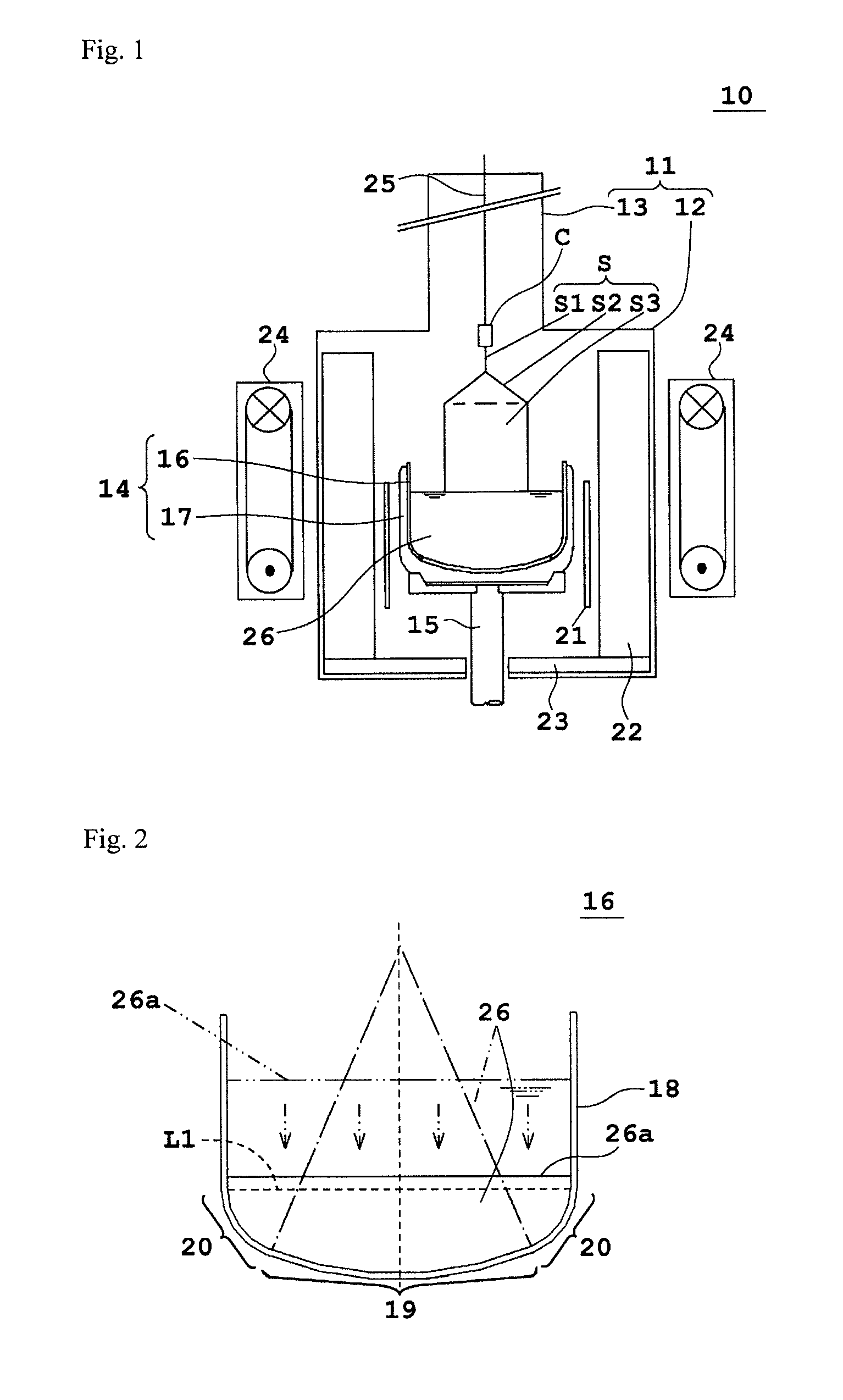
[0058]A crystal growth apparatus 10 in FIG. 1 is used in the silicon monocrystal growth method according to the first embodiment. The crystal growth apparatus 10 has a hollow cylindrical chamber 11. The chamber 11 has a main chamber 12 and a pull chamber 13, which is connectedly fixed onto the main chamber 12 and has a smaller diameter than the main chamber 12. In a central portion of the main chamber 12, a crucible 14 is fixed onto a rotatable and vertically movable support axis (pedestal) 15. The crucible 14 has a double structure combining an internal quartz crucible 16 and an external graphite crucible 17. The quartz crucible 16 includes a peripheral wall portion 18 having a constant external diameter, and a bulging bottom portion 19 provided below the peripheral wall portion 18 and provided with an external surface having a predetermined curvature radius (100% of the external diameter of the peripheral wall portion). The peripheral wall portion 18 and the bottom portion 19 are ...


PUM


Abstract

Silicon monocrystal growth is ended before a liquid surface of a melt reaches a corner portion of a quartz crucible, and thus dislocation of a silicon monocrystal can be reduced and reduction in yield can be prevented.

Description

BACKGROUND OF THE INVENTION[0001]1. Field of the Invention[0002]The present invention relates to a silicon monocrystal growth method, specifically a silicon monocrystal growth method capable of reducing an occurrence ratio of dislocation in a silicon monocrystal.[0003]2. Description of Related Art[0004]When a silicon monocrystal is produced in a Czochralski process (CZ process), solid silicon material is heated and melted in a quartz crucible, and thereby a melt (silicon melt) is formed. Subsequently, a seed crystal is immersed in the melt, and then pulled up while being rotated. Thereby, a silicon monocrystal is grown beneath the seed crystal (Related Art 1, for example). The seed crystal used herein has a diameter of several tens mm or less. In a general crystal growth method, a diameter is increased from a neck portion to a predetermined diameter greater than the diameter of the seed crystal (diameter increasing portion). Thereafter, a straight body portion (body portion) is form...

Claims


Application Information

Patent Timeline
IPC IPC(8): C30B15/30C30B15/10
CPCC30B29/06C30B15/20
Inventor FUJIWARA, TOSHIYUKIHOSOI, TAKEHIKONAKAMURA, TSUYOSHI
Owner SUMCO CORP
Learn More