Light-Emitting Element, Light-Emitting Device, and Method for Manufacturing the Same
- Summary
- Abstract
- Description
- Claims
- Application Information
AI Technical Summary
Benefits of technology
Problems solved by technology
Method used
Image
Examples
embodiment 1
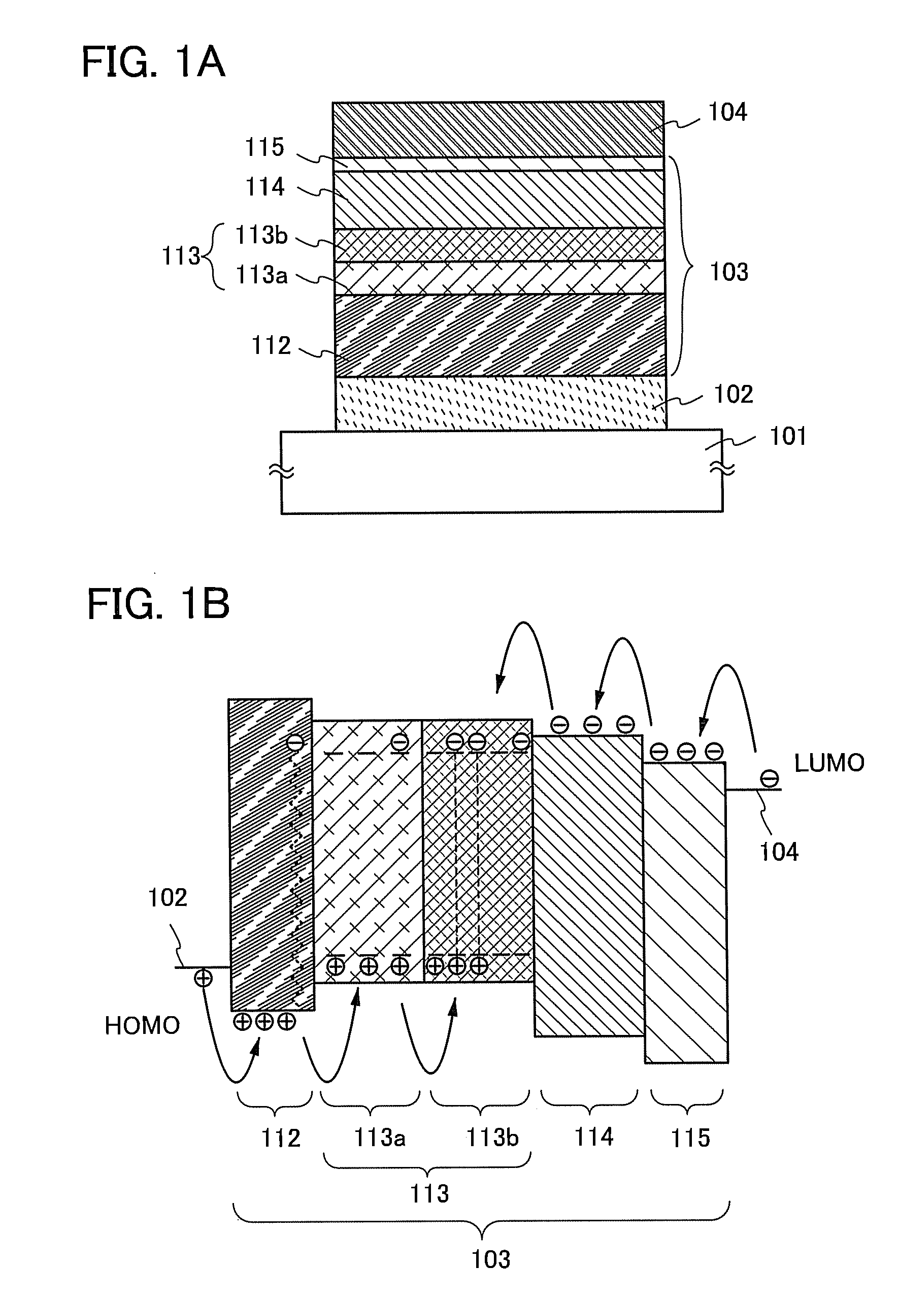
[0050]A light-emitting element which is illustrated in Embodiment 1 includes at least a first light-emitting layer whose one side is in contact with a hole-transport layer and a second light-emitting layer which is in contact with the other side of the first light-emitting layer. The first light-emitting layer and the second light-emitting layer each include a bipolar host material and a guest material which is a light-emitting substance, and the hole-transport property of the first light-emitting layer is higher than that of the second light-emitting layer. Further, an anti-reducing substance is included in the hole-transport layer so that the hole-transport layer is not reduced by electrons passing through the light-emitting layer and reaching the hole-transport layer.
[0051]FIG. 1A illustrates the structure of the light-emitting element of Embodiment 1. The light-emitting element of Embodiment 1 includes a first electrode 102, a second electrode 104, and an EL layer 103. The first...
embodiment 2
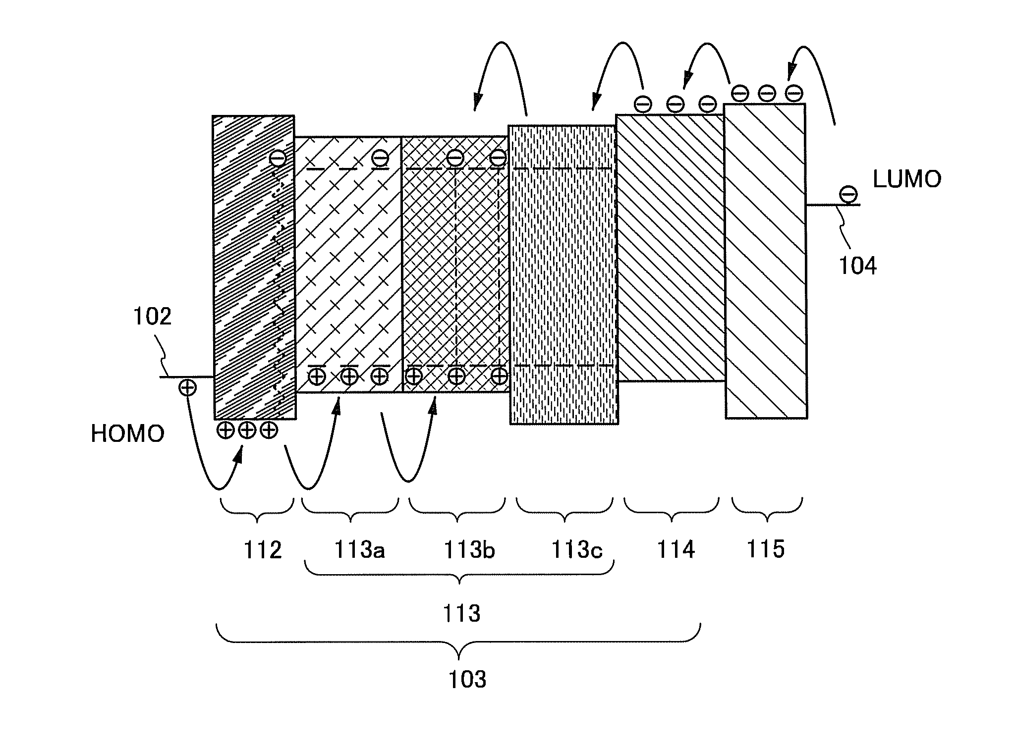
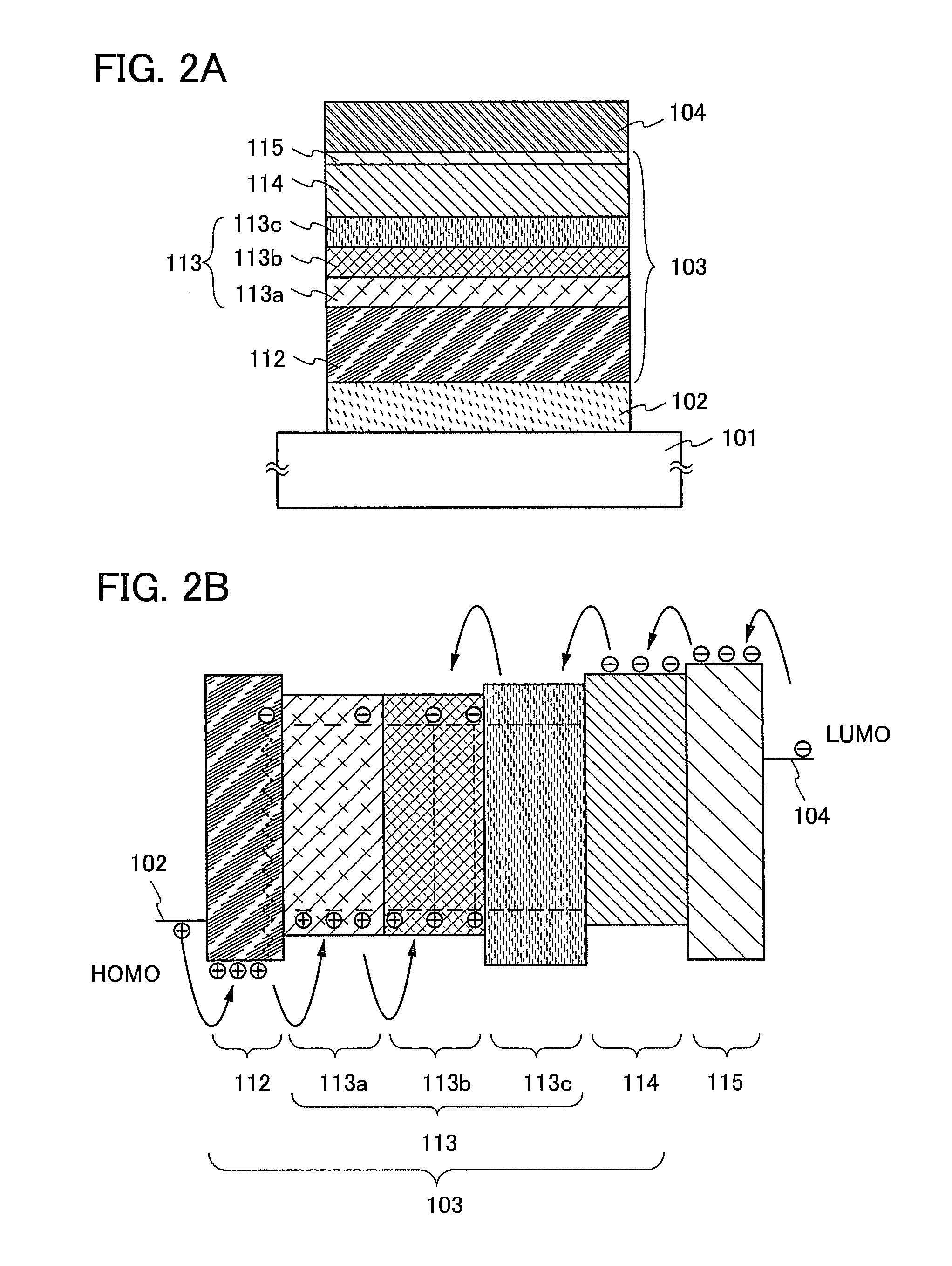
[0138]A light-emitting layer included in a light-emitting element which is illustrated in Embodiment 2 includes a first light-emitting layer in contact with a hole-transport layer, a second light-emitting layer in contact with the first light-emitting layer, and a third light-emitting layer in contact with the second light-emitting layer. The first light-emitting layer and the second light-emitting layer each include a bipolar host material and a guest material which is a light-emitting substance, and the hole-transport property of the first light-emitting layer is higher than that of the second light-emitting layer. The third light-emitting layer prevents holes from being injected from the light-emitting layer to an electron-transport layer. Further, an anti-reducing substance is included in the hole-transport layer so that the hole-transport layer is not reduced by electrons passing through the light-emitting layer and reaching the hole-transport layer.
[0139]FIG. 2A illustrates th...
embodiment 3
[0151]In Embodiment 3, a light-emitting device manufactured using a light-emitting element of an embodiment of the present invention is described with reference to FIGS. 12A and 12B and FIGS. 13A and 13B. Note that FIG. 12A is a top view illustrating the light-emitting device and FIG. 12B is a cross-sectional view of FIG. 12A taken along a line A-A′. Reference numeral 401 shown by a dotted line denotes a driver circuit portion (a source side driver circuit); reference numeral 402 denotes a pixel portion; and reference numeral 403 denotes a driver circuit portion (a gate side driver circuit). Reference numeral 404 denotes a sealing substrate; reference numeral 405 denotes a sealant; and an inner side region enclosed by the sealant 405 is a space 407.
[0152]Note that a lead wiring 408 is a wiring for transmitting signals that are to be inputted to the source side driver circuit 401 and the gate side driver circuit 403, and receives a video signal, a clock signal, a start signal, a rese...
PUM
 Abstract
Description
Claims
Application Information
 - R&D
- Intellectual Property
- Life Sciences
- Materials
- Tech Scout
- Unparalleled Data Quality
- Higher Quality Content
- 60% Fewer Hallucinations
Browse by: Latest US Patents, China's latest patents, Technical Efficacy Thesaurus, Application Domain, Technology Topic, Popular Technical Reports.
© 2025 PatSnap. All rights reserved.Legal|Privacy policy|Modern Slavery Act Transparency Statement|Sitemap|About US| Contact US: help@patsnap.com


