
Thin film type solar cell and method for manufacturing the same

Inactive Publication Date: 2010-10-07
JUSUNG ENG
View PDF10 Cites 14 Cited by
  • Summary
  • Abstract
  • Description
  • Claims
  • Application Information

AI Technical Summary

Benefits of technology

[0051]The thin film type solar cell according to the present invention and the method for manufacturing the same has the following advantages.
[0052]In the related art method for manufacturing the thin film type solar cell, large amount of particles are generated due to performance of laser-scribing procedures. However, the method for manufacturing the thin film type solar cell according to the present invention doesn't require the laser-scribing procedure, whereby the particles are not generated in the method for manufacturing the thin film type solar cell according to the present invention. As a result, the method for manufacturing the thin film type solar cell according to the present invention can avoid various problems caused by the particles, for example, contamination of the substrate, short of the device, scribing for the undesired layer, the complicated process, and impossibility of performing the consecutive procedure.
[0053]According as the thin film type solar cell according to the present invention is divided into the plurality of unit cells through the use of auxiliary electrode or partition wall instead of the related art laser-scribing method, it is possible to prevent the resistance of front electrode layer from being increased even in the large-sized device.
[0054]Also, the insulating layer as well as the auxiliary electrode is formed additionally, thereby preventing the problems generated in the interface between the auxiliary electrode and the semiconductor layer, and realizing the precise division in the solar cell. Additionally, the insulating layer makes it possible to increase the entire size of the semiconductor layer and improve the light-capturing efficiency.

Problems solved by technology

However, in the case of the wafer type solar cell, it is difficult to realize a small thickness due to difficulty in performance of the manufacturing process.
In addition, the wafer type solar cell uses a high-priced semiconductor substrate, whereby its manufacturing cost is increased.
With the large-sized substrate, a resistance is increased in the front electrode made of the transparent conductive material, thereby causing the increase in power loss.
However, the related art method for manufacturing the thin film type solar cell necessarily requires the laser-scribing procedure.
First, large amounts of particles may generate due to the performance of laser-scribing procedure. The generated particles may cause the problems such as a contamination of substrate and a short of device.
Second, if laser is excessively supplied to the desired layer due to the inappropriate control of laser irradiation and exposing time, the lower layer positioned underneath the desired layer as well as the desired layer may be scribed together.
Third, the laser-scribing procedure may cause the complicacy in the process for manufacturing the thin film type solar cell. In addition, it is difficult to perform the laser-scribing procedure maintained under atmospheric conditions and other procedures maintained under vacuum conditions in succession.

Method used


Image

  • Thin film type solar cell and method for manufacturing the same
  • Thin film type solar cell and method for manufacturing the same
  • Thin film type solar cell and method for manufacturing the same

Examples


first embodiment

[0139]FIGS. 12A to 12E are cross section views illustrating a method for manufacturing a thin film type solar cell according to the first embodiment of the present invention.

[0140]First, as shown in FIG. 12A, the front electrode layer 200 is formed on the substrate 100.

[0141]At this time, the substrate 100 may be formed of glass or transparent plastic. The transparent conductive layer 200 may be formed of the transparent conductive material such as ZnO, ZnO:B, ZnO:Al, ZnO:H, SnO2, SnO2:F, or ITO (Indium Tin Oxide) by sputtering or MOCVD (Metal Organic Chemical Vapor Deposition).

[0142]The front electrode layer 200 may have the uneven surface through the texturing process.

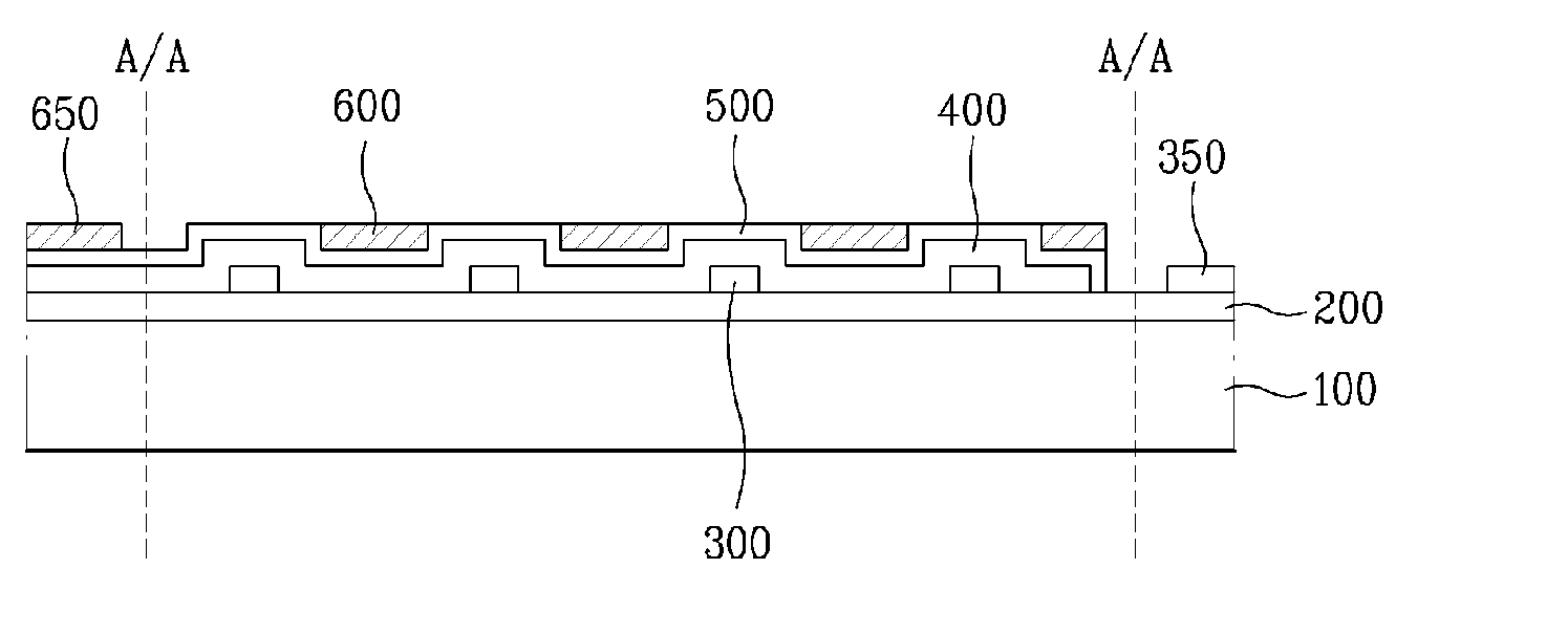
[0143]As shown in FIG. 12B, the auxiliary electrode 300 is formed on the front electrode layer 200.

[0144]The auxiliary electrode 300 and the first bus line 350 are formed at the same time. At this time, the auxiliary electrode 300 is formed within the active area (A / A) of the thin film type solar cell, and the first ...

second embodiment

[0155]FIGS. 13A to 13F are cross section views illustrating a method for manufacturing a thin film type solar cell according to the second embodiment of the present invention.

[0156]First, as shown in FIG. 13A, the front electrode layer 200 is formed on the substrate 100.

[0157]Then, as shown in FIG. 13B, the auxiliary electrode 300 and the first bus line 350 connected with the auxiliary electrode 300 are formed on the front electrode layer 200.

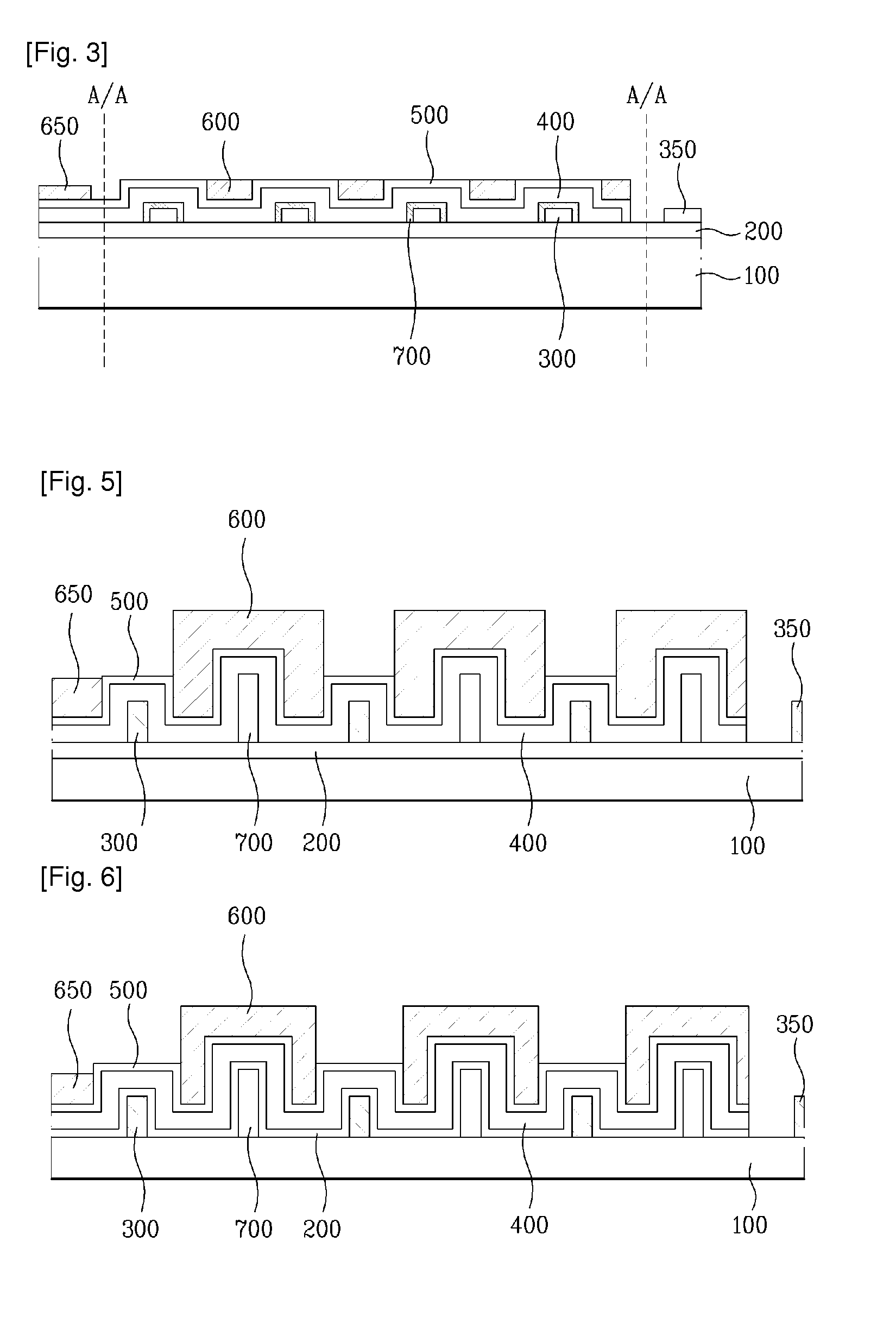
[0158]As shown in FIG. 13C, the insulating layer 700 covers the auxiliary electrode 300, that is, the insulating layer 700 is formed on the lateral and upper surfaces of the auxiliary electrode 300.

[0159]In more detail, the insulating layer 700 is formed on the lateral and upper surfaces of first auxiliary electrode 310, second auxiliary electrodes 320a, 320b, 320c and 320d, and third auxiliary electrode 330 shown in FIGS. 8A to 8D.

[0160]The insulating layer 700 may be formed of the insulating material such as SiO2, TiO2, SiNx, SiON, or polymer...

third embodiment

[0165]FIGS. 14A to 14F are cross section views illustrating a method for manufacturing a thin film type solar cell according to the third embodiment of the present invention.

[0166]First, as shown in FIG. 14A, the front electrode layer 200 is formed on the substrate 100.

[0167]Next, as shown in FIG. 14B, the insulating layer 700 is formed on the front electrode layer 200.

[0168]The insulating layer 700 is positioned at one side of the auxiliary electrode formed during the procedure of FIG. 14C. At this time, the insulating layer 700 is formed such that the insulating layer 700 becomes higher than the auxiliary electrode 300.

[0169]As shown in FIG. 14C, the auxiliary electrode 300 and the first bus line 350 connected with the auxiliary electrode 300 are formed on the front electrode layer 200.

[0170]The auxiliary electrode 300 is positioned next to the insulating layer 700.

[0171]In the meantime, the auxiliary electrode 300 and the first bus line 350 are firstly formed, and then the insula...


PUM


Abstract

A thin film type solar cell and a method for manufacturing the same is disclosed, which can overcome various problems caused by a related art laser-scribing procedure since the thin film type solar cell is divided into a plurality of sub-cells through the use of auxiliary electrode or partition wall, the thin film type solar cell comprising a substrate; a front electrode layer and a cell-dividing part on the substrate; and a rear electrode on the semiconductor layer.

Description

TECHNICAL FIELD[0001]The present invention relates to a thin film type solar cell, and more particularly, to a thin film type solar cell which is suitable for minimizing a resistance of front electrode.BACKGROUND ART[0002]A solar cell with a property of semiconductor converts a light energy into an electric energy.[0003]A structure and principle of the solar cell according to the related art will be briefly explained as follows. The solar cell is formed in a PN-junction structure where a positive(P)-type semiconductor makes a junction with a negative(N)-type semi-conductor. When a solar ray is incident on the solar cell with the PN-junction structure, holes(+) and electrons(−) are generated in the semiconductor owing to the energy of solar ray. By an electric field generated in an PN-junction area, the holes(+) are drifted toward the P-type semiconductor, and the electrons(−) are drifted toward the N-type semiconductor, whereby an electric power is produced with an occurrence of ele...

Claims


Application Information

Patent Timeline
IPC IPC(8): H01L31/00
CPCH01L31/022425H01L31/022433H01L31/0463H01L31/1804Y02E10/547H01L31/03921Y02P70/50
Inventor HONG, JINKIM, JAE HOKIM, JOUNG SIK
Owner JUSUNG ENG
Learn More