Thermal tuning of an optical device

a technology of optical waveguide and thermal tuning, which is applied in the direction of optical waveguide light guide, instruments, optics, etc., can solve the problems of degrading the quality factor of an optical resonator, introducing additional optical losses, and affecting the so as to facilitate thermal tuning of optical waveguides and reduce optical waveguide losses. , the effect of reducing optical waveguide losses

Active Publication Date: 2010-09-30
ORACLE INT CORP
View PDF10 Cites 30 Cited by
  • Summary
  • Abstract
  • Description
  • Claims
  • Application Information

AI Technical Summary

Benefits of technology

[0016]Doping of the semiconductor layer in the optical waveguide may define a heater that facilitates thermal tuning of the optical waveguide. Moreover, power consumption by the heater may be less than 10-20 mW for a 180° phase shift in the optical waveguide. In some embodiments, the doping of the semiconductor layer in the optical waveguide alternates between a first type of region and a second type of region along an axis of the optical waveguide (such as a symmetry axis or a principal axis), where the first type of region has a lower doping of the semiconductor layer than the second type of region, thereby reducing optical losses in the optical waveguide.
[0017]Note that the doping of the semiconductor layer in a central region of the optical waveguide may be less than the doping of the semiconductor layer in a lateral region surrounding the optical waveguide, thereby reducing optical losses in the optical waveguide. Furthermore, the optical waveguide may include a top portion and a bottom portion, and the semiconductor layer may only be doped in the bottom portion of the optical waveguide, thereby reducing optical losses in the optical waveguide.
[0018]In some embodiments, portions of the electrodes may have a lower thermal conductivity than a remainder of the electrodes, thereby reducing the power consumption associated with thermal tuning of the optical waveguide by reducing thermal coupling from an external environment to the optical waveguide. These portions of the electrodes may include indium-tin-oxide (or another material with a high electrical conductivity and a low thermal conductivity).
[0019]In some embodiments, the electrodes are configured to reduce heat flow in a plane of the optical waveguide along a direction approximately perpendicular to the axis of the optical waveguide. For example, the electrodes may be thermally coupled to the optical waveguide by multiple regions in the semiconductor layer which have a higher thermal conductivity than additional regions that are interdigited with the regions. Moreover, a given region may have an axis (such as a symmetry axis or principal axis) that is approximately perpendicular to the axis of the optical waveguide in a plane of the semiconductor layer (for example, within 15° of perpendicular). Note that doping of the semiconductor layer in the given region may exceed doping of the semiconductor in the optical waveguide, thereby reducing power consumption associated with thermal tuning of the optical waveguide by reducing thermal coupling from an external environment to the optical waveguide. For example, the doping of the semiconductor layer in the regions may be at least 10 times larger than the doping of the semiconductor layer in the optical waveguide. Additionally, a width of the given region may be at least five times smaller than a periodicity of the regions along the axis of the optical waveguide.

Problems solved by technology

Typically, the direct-heating technique is more energy-efficient than indirect heating, but it can prevent the optical waveguide from performing additional functions (because of the constraint on the doping density), and it can introduce additional optical losses due to free-carrier absorption (which can degrade the quality factor of an optical resonator).
Unfortunately, there are problems associated with silicon-based optical devices.
A notable problem is the high thermal conductivity of silicon.
While this helps remove the heat dissipated by electrical circuits, it can make it more difficult to thermally tune a silicon-based optical device.
However, the high thermal conductivity of silicon results in excessive thermal coupling to the surrounding environment.
Consequently, thermal tuning of silicon-based optical devices often consumes a disproportionately large amount of energy (typically, 50-100 mW for a phase shift of 180°).
This high power consumption can offset the advantages provided by silicon, and makes it more difficult to use silicon-based optical devices to implement optical communication (such as WDM) in computing systems (especially in systems that have multiple instances of the optical devices).

Method used


Image

  • Thermal tuning of an optical device
  • Thermal tuning of an optical device
  • Thermal tuning of an optical device

Examples


Embodiment Construction

[0033]The following description is presented to enable any person skilled in the art to make and use the invention, and is provided in the context of a particular application and its requirements. Various modifications to the disclosed embodiments will be readily apparent to those skilled in the art, and the general principles defined herein may be applied to other embodiments and applications without departing from the spirit and scope of the present invention. Thus, the present invention is not intended to be limited to the embodiments shown, but is to be accorded the widest scope consistent with the principles and features disclosed herein.

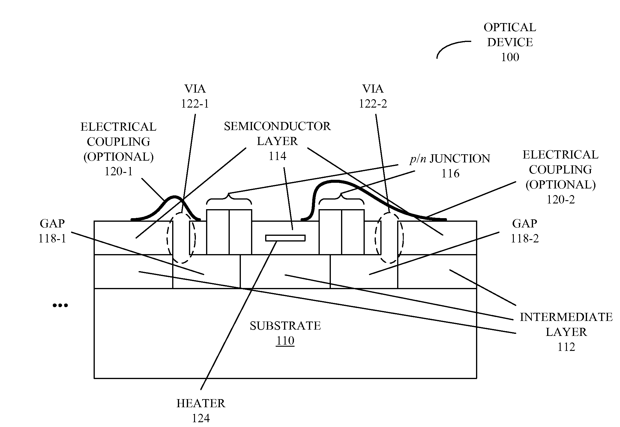
[0034]Embodiments of an optical device, an array of optical devices, and a technique for fabricating the optical device or the array are described. This optical device is implemented on a substrate (such as silicon), and includes a thermally tunable optical waveguide with a high thermal resistance to the surrounding external environment and a l...


PUM


Abstract

Embodiments of an optical device, an array of optical devices, and a technique for fabricating the optical device or the array are described. This optical device is implemented on a substrate (such as silicon), and includes a thermally tunable optical waveguide with a high thermal resistance to the surrounding external environment and a low thermal resistance to a localized heater. In particular, the thermal resistances associated with thermal dissipation paths from a heater in the optical device to an external environment via electrodes and via the substrate are increased, while the thermal resistance between the optical waveguide and the heater is decreased.

Description

CROSS REFERENCE TO RELATED APPLICATIONS[0001]This application is related to U.S. patent application Serial Number, not yet assigned, entitled “Optical Device with Large Thermal Impedance,” by John E. Cunningham, Ashok V. Krishnamoorthy, Ivan Shubin, Guoliang Li and Xuezhe Zheng, (attorney docket number SUN09-0005) filed on 31 Mar., 2009; and to U.S. patent application Serial Number, not yet assigned, entitled “Dual-Layer Thermally Tuned Optical Device,” by Guoliang Li, John E. Cunningham, Ashok V. Krishnamoorthy, Ivan Shubin and Xuezhe Zheng, (attorney docket number SUN09-0014) filed on 31 Mar. 2009, the contents of each of which are herein incorporated by reference.GOVERNMENT LICENSE RIGHTS[0002]This invention was made with Government Support under Agreement No. HR0011-08-9-0001 awarded by DARPA. The Government has certain rights in the invention.BACKGROUND[0003]1. Field of the Invention[0004]The present invention relates to techniques for communicating optical signals. More specif...

Claims


Application Information

Patent Timeline
Patent Type & Authority Applications(United States)
IPC IPC(8): G02B6/12
CPCG02B6/12007G02B2006/12061G02F2202/10G02F1/0147G02F1/011
Inventor LI, GUOLIANGKRISHNAMOORTHY, ASHOK V.CUNNINGHAM, JOHN E.SHUBIN, IVANZHENG, XUEZHE
Owner ORACLE INT CORP
Why Eureka
Try Eureka