Display device and manufacturing method thereof

a technology of a display device and a manufacturing method, which is applied in the manufacture of electric discharge tubes/lamps, instruments, and the association of printed circuit non-printed electric components, etc., can solve the problems of unsuitable adhesive for repair, and achieve the effects of preventing interference, easy repair, and uniform attachmen

Active Publication Date: 2010-06-03
PANASONIC LIQUID CRYSTAL DISPLAY CO LTD +1
View PDF13 Cites 35 Cited by
  • Summary
  • Abstract
  • Description
  • Claims
  • Application Information

AI Technical Summary

Benefits of technology

[0008]It is an object of the invention to provide a display device that prevents interference between a light transmissive substrate and a circuit board by providing a sufficient gap between the circuit board and the light transmissive substrate and enables uniform attachment of the light transmissive substrate to the circuit board.
[0009]It is another object of the invention to provide a display device that is easily repaired.
[0010](1) A display device according to the invention includes: a display panel; a light transmissive circuit board attached to a display face of the display panel; a light transmissive substrate disposed on the opposite side of the circuit board from the display panel so as to face the circuit board; a mounted component mounted on the circuit board such that at least a part of the mounted component is intervened between the circuit board and the light transmissive substrate; and a light transmissive junction layer joining the circuit board to the light transmissive substrate at a position avoiding the mounted component, wherein the junction layer includes a core substrate formed of a resin, an adhesive layer formed on one face of the core substrate, and a bonding layer formed on the other face of the core substrate and cured, the adhesive layer is adhered to one of the circuit board and the light transmissive substrate, and the bonding layer is firmly fixed to the other of the circuit board and the light transmissive substrate. According to the invention, a sufficient gap can be provided between the circuit board and the light transmissive substrate because the core substrate is intervened therebetween, and repair of the light transmissive substrate can be easily performed because the adhesion interface can be separated.
[0012](3) A method for manufacturing a display device according to the invention includes the steps of: preparing a display panel, a light transmissive circuit board having a mounted component mounted thereon, a light transmissive substrate, and a core substrate formed of a light transmissive resin; attaching the circuit board to a display face of the display panel; adhering the core substrate to one of the circuit board and the light transmissive substrate via an adhesive layer; and bonding the other of the circuit board and the light transmissive substrate to the core substrate adhered to the one of the circuit board and the light transmissive substrate with an adhesive, wherein the step of bonding with the adhesive is performed such that at least a part of the mounted component is intervened between the circuit board and the light transmissive substrate. According to the invention, it is possible to provide a sufficient gap between the circuit board and the light transmissive substrate, prevent interference in a difference of level of the circuit board, and uniformly attach the circuit board to the light transmissive substrate because the core substrate is intervened. In addition, since the adhesion interface can be separated, the light transmissive substrate can be easily repaired.

Problems solved by technology

When a sufficient gap is not formed between the circuit board and the light transmissive substrate like the related art described above, it has been found that there arises a problem of interference between a print layer formed on the light transmissive substrate and the circuit board.
In addition, there is also another problem that the adhesive is not suitable for repair because it firmly bonds.

Method used


Image

  • Display device and manufacturing method thereof
  • Display device and manufacturing method thereof

Examples


Embodiment Construction

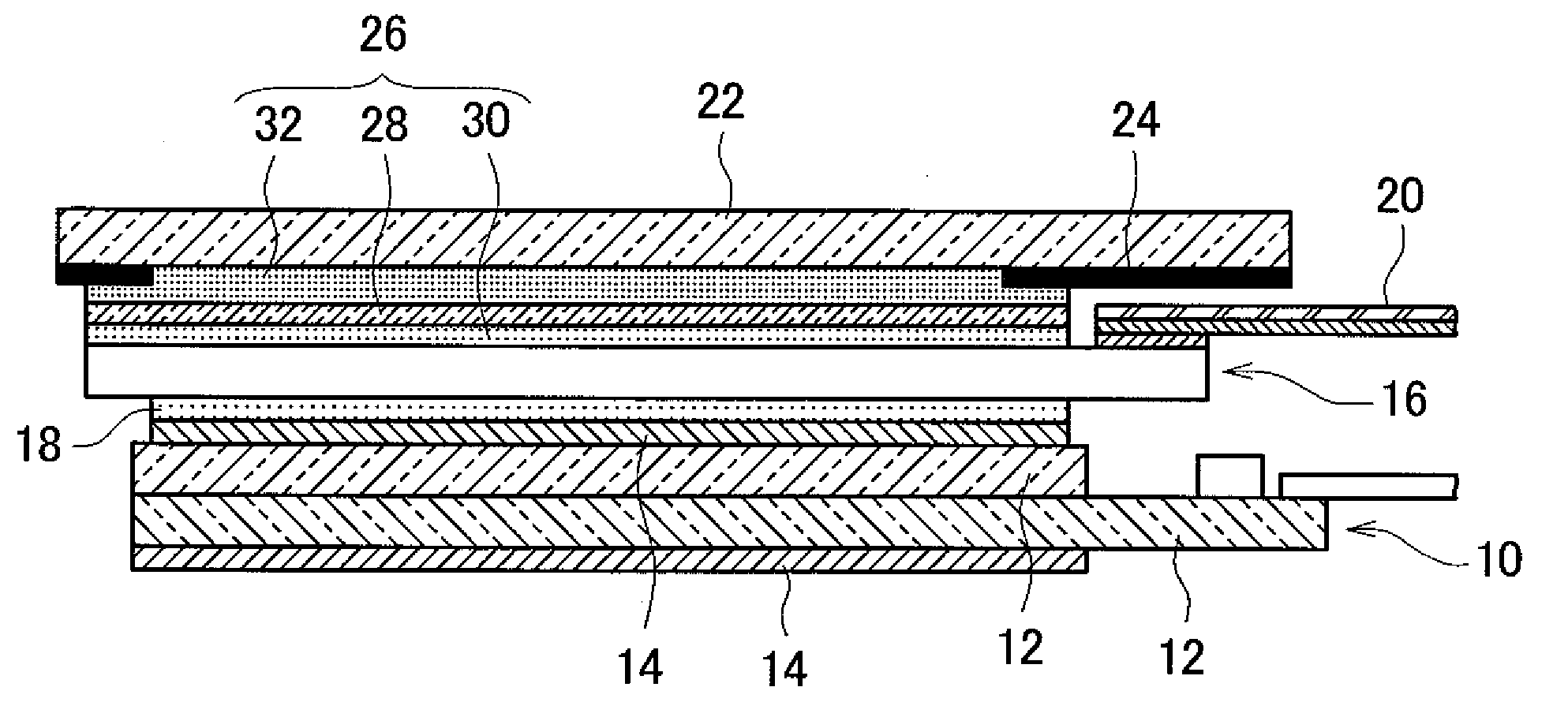
[0017]The object of the invention is to provide a display device in which a sufficient gap is provided between a circuit board and a light transmissive substrate and that can be repaired. The display device of the invention includes a display panel attached to one face (first face of the circuit board) side of the light transmissive circuit board and the light transmissive substrate attached to the other face (second face of the circuit board) side of the circuit board. The circuit board has a mounted component mounted on the other face (second face of the circuit board) side. The circuit board includes a light transmissive junction layer for joining the circuit board to the light transmissive substrate at a position avoiding the mounted component. The junction layer includes a core substrate formed of a resin, an adhesive layer formed on one face (first face of the core substrate) of the core substrate, and a bonding layer formed on the other face (second face of the core substrate...


PUM


Abstract

A display device of the invention includes a display panel attached to one face side of a light transmissive circuit board and a light transmissive substrate attached to the other face side of the circuit board. A mounted component is mounted on the other face side of the circuit board. The circuit board includes a light transmissive junction layer for joining the circuit board to the light transmissive substrate at a position avoiding the mounted component. The junction layer includes a core substrate formed of a resin, an adhesive layer formed on one face of the core substrate, and a bonding layer formed on the other face of the core substrate and cured. The adhesive layer is adhered to the circuit board, and the bonding layer is firmly fixed to the light transmissive substrate.

Description

CROSS-REFERENCE TO RELATED APPLICATION[0001]The present application claims priority from Japanese application JP 2008-297655 filed on Nov. 21, 2008, the content of which is hereby incorporated by reference into this application.BACKGROUND OF THE INVENTION[0002]1. Field of the Invention[0003]The present invention relates to a display device and a manufacturing method thereof.[0004]2. Description of Related Art[0005]Display panels, such as liquid crystal display panels or organic electroluminescence panels, having a circuit board such as a touch panel attached thereto have been known. A light transmissive substrate is attached to the circuit board. In this case, the circuit board and the light transmissive substrate are both rigid bodies. It is difficult to remove air bubbles when a pressure-sensitive adhesive double coated sheet is used for attaching them together, and therefore an adhesive is used for attachment. Since a mounted component such as a flexible wiring board or an integr...

Claims


Application Information

Patent Timeline
Patent Type & Authority Applications(United States)
IPC IPC(8): G06F3/044H05K7/00H01J9/20
CPCG06F3/044G06F3/0416G06F3/0412
Inventor ITO, HIROSHIOJIMA, KAZUNORIABE, HIDEAKITANABE, SHINJIYANAGIHARA, MASAYUKI
Owner PANASONIC LIQUID CRYSTAL DISPLAY CO LTD
Why Eureka
Try Eureka