
Method for performing an electrical testing of electronic devices

a technology for electronic devices and electrical testing, applied in electrical testing, measurement devices, instruments, etc., can solve problems such as electrical yield loss, complicated further device assembly, and difficulty in performing electrical testing of complex on-wafer duts using this kind of method

Active Publication Date: 2010-06-03
STMICROELECTRONICS SRL
View PDF20 Cites 39 Cited by
  • Summary
  • Abstract
  • Description
  • Claims
  • Application Information

AI Technical Summary

Benefits of technology

[0026]The solution being described in the above-mentioned article is effective for mixed-signal DUTs with a low content of analog circuits, while it could be hardly applied to mixed-signal DUTs with a considerable ...

Problems solved by technology

The testing of complex on-wafer DUTs performed by using this kind of method is considerably complicated since several testing operations generally should be performed and the wafer should be thus necessarily contacted several times.
Moreover, the use of probes connecting the ATE with the wafer often involves the damaging of the selected device pads, complicating the further device assembly.
Furthermore, performing the testing of several parallel-connected DUT requires the use of probe cards with a very high number of probes, increasing contacting problems and thus of electrical continuity between the probes of the probe card and the DUT pads and also causing problems of electrical yield loss.
It should be also said that the number of ATE resources to be used increases according to the number of pads to be contacted on the DUT to be tested and, consequently, the number of DUTs which can be tested in parallel decreases, inevitably increasing testing costs.
Consequently, the electrical selection process is considerably complicated.
In fact, for complex DUT testing, it is necessary to have ATEs of different type and high cost, besides solving production problems due to the analog and RF circuits in the DUT.
This technique thus requires the availability in the ATE of expensive and complex resources, being necessary to store and apply input test vectors and then to compare them with the expected results.
Consequently, in order to allow these LPC testing interfaces to be used it is necessary to insert, in the device, dedicated circuits which disadvantageously occupy a certain device area.
The disadvantage of the structure created by BIST circuits is the unsuitable performance in terms of failure coverage in the case of a generic circuit which can be not completely digital.
Nevertheless, disadvantageously, for performing the testing of non volatile memories (NVM), for example of the flash type, it is necessary to perform two testing flows, since also the retention test of Floating Gate Avalance Metal Oxide Semiconductor (FAMOS) memory cells should be performed.
Nevertheless, a disadvantage of this king of testing is that mixed-signal ATEs have a cost which is generally very high and anyhow higher than other kinds of ATE.
Nevertheless, performing this kind of testing has several problems.
For DUTs comprising circuits of the analog and / or RF type, it is very difficult to reduce the number of resources to be contacted, and it is usually necessary to connect the DUT with all ATE resources referring to these circuits.
Consequently, ATEs being used are considerably complex and very expensive.
Moreover, the presence of analog and RF circuits in the DUT makes the testing difficult because of the several parasitic phenomena in the electrical measurement chain between the DUT and ATE internal instruments.
Thus, finding out a standard testing approach, able to reduce the number of ATEs of different kind to be used for the testing and, consequently, the costs, the complexity of testing flows and of the productive process in general, is a big problem.
The solution being described in the above-mentioned article is effective for mixed-signal DUTs with a low content of analog circuits, while it could be hardly applied to mixed-signal DUTs with a considerable analog part since, in this case, the DIB board would become very complex and expensive.
Moreover, the DIB board being described is a dedicated interface to the specific DUT, generally not reusable for other kinds of DUT.

Method used


Image

  • Method for performing an electrical testing of electronic devices
  • Method for performing an electrical testing of electronic devices
  • Method for performing an electrical testing of electronic devices

Examples


Embodiment Construction

[0156]In the following description, certain details are set forth in order to provide a thorough understanding of various embodiments of devices, methods and articles. However, one of skill in the art will understand that other embodiments may be practiced without these details. In other instances, well-known structures and methods associated with DUTs, ATEs and control systems have not been shown or described in detail to avoid unnecessarily obscuring descriptions of the embodiments.

[0157]Unless the context requires otherwise, throughout the specification and claims which follow, the word “comprise” and variations thereof, such as “comprising,” and “comprises,” are to be construed in an open, inclusive sense, that is, as “including, but not limited to.”

[0158]Reference throughout this specification to “one embodiment,” or “an embodiment” means that a particular feature, structure or characteristic described in connection with the embodiment is included in at least one embodiment. Th...


PUM


Abstract

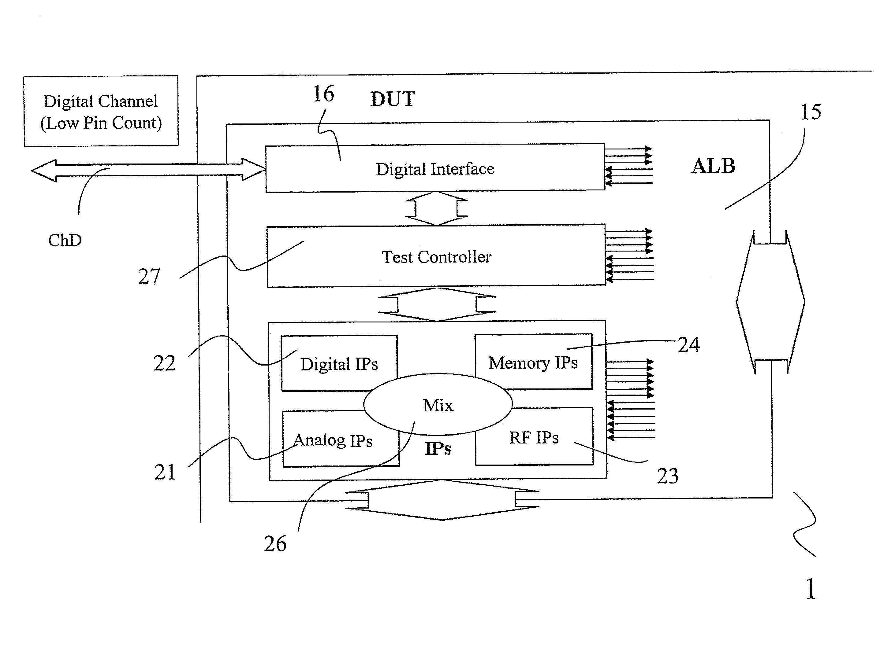
A method of electrical testing electronic devices DUT, comprising: connecting at least an electronic device DUT to an automatic testing apparatus suitable for performing the testing of digital circuits or memories or of digital circuits and memories; sending electrical testing command signals to the electronic device DUT by means of the ATE apparatus; performing electrical testing of the electronic device DUT by means of at least one advanced supervised self testing system “Advanced Low Pin Count BIST” ALB which is built in the electronic device DUT, the ALB system being digitally interfaced with the ATE through a dedicated digital communication channel; and sending reply messages, if any, which comprise measures, failure information and reply data to the command signals from the electronic device DUT toward the ATE apparatus by means of the digital communication channel.

Description

BACKGROUND[0001]1. Technical Field[0002]The present disclosure relates to methods for performing an electrical testing of electronic devices.[0003]The present disclosure also relates to systems for performing the electrical testing of electronic devices.[0004]2. Description of the Related Art[0005]At present to perform an electrical wafer sort (EWS) testing of an electronic device to be tested or Device Under Testing (DUT), it is necessary to electrically connect a testing apparatus or tester, such as an Automatic Test Equipment (ATE), with the wafer comprising a plurality of electronic components to be selected. In particular, a probe card is used, comprising at least one probe or more generally a plurality of probes, acting as an interface between the ATE and the wafer. The probe card is a board comprising a printed circuit or Printed Circuit Board (PCB) and several dozens (often even several hundreds) of probes which electrically connect the ATE with most of the electrical termin...

Claims


Application Information

Patent Timeline
IPC IPC(8): G01R31/02
CPCG01R31/31713
Inventor PAGANI, ALBERTO
Owner STMICROELECTRONICS SRL
Learn More