
Thermoelectric device, thermoelectic device module, and method of forming the thermoelectric device

a technology of thermoelectric devices and modules, applied in the field of thermoelectric devices, can solve the problems of low mechanical strength of thermoelectric devices including bisub>2/sub>tesub>3 /sub>, environmental pollution, and difficult recycling of thermoelectric devices including bisub>2/sub>tesub>3

Inactive Publication Date: 2010-05-27
ELECTRONICS & TELECOMM RES INST
View PDF6 Cites 43 Cited by
  • Summary
  • Abstract
  • Description
  • Claims
  • Application Information

AI Technical Summary

Benefits of technology

[0023]In yet much further embodiments, the semiconductor nanowire and the second

Problems solved by technology

However, heavy metals are used for the thermoelectric devices including Bi2Te3, and the thermoelectric devices including Bi2Te3 are very difficult to recycle.
In addition, the thermoelectric devices including Bi2Te3 may cause environmental pollution.
Furthermore, the thermoelectric devices including Bi2Te3 have a low mechanical strength, and are difficult to miniaturize and very susceptible to moisture damage.

Method used


Image

  • Thermoelectric device, thermoelectic device module, and method of forming the thermoelectric device
  • Thermoelectric device, thermoelectic device module, and method of forming the thermoelectric device
  • Thermoelectric device, thermoelectic device module, and method of forming the thermoelectric device

Examples


Embodiment Construction

[0033]Preferred embodiments of the present invention will be described below in more detail with reference to the accompanying drawings. The present invention may, however, be embodied in different forms and should not be constructed as limited to the embodiments set forth herein. Rather, these embodiments are provided so that this disclosure will be thorough and complete, and will fully convey the scope of the present invention to those skilled in the art.

[0034]In the figures, the dimensions of layers and regions are exaggerated for clarity of illustration. It will also be understood that when a layer is referred to as being ‘on’ another layer or substrate, it can be directly on the other layer or substrate, or intervening layers may also be present. Further, it will be understood that when a layer is referred to as being ‘under’ another layer, it can be directly under, and one or more intervening layers may also be present. In addition, it will also be understood that when a layer...


PUM


Abstract

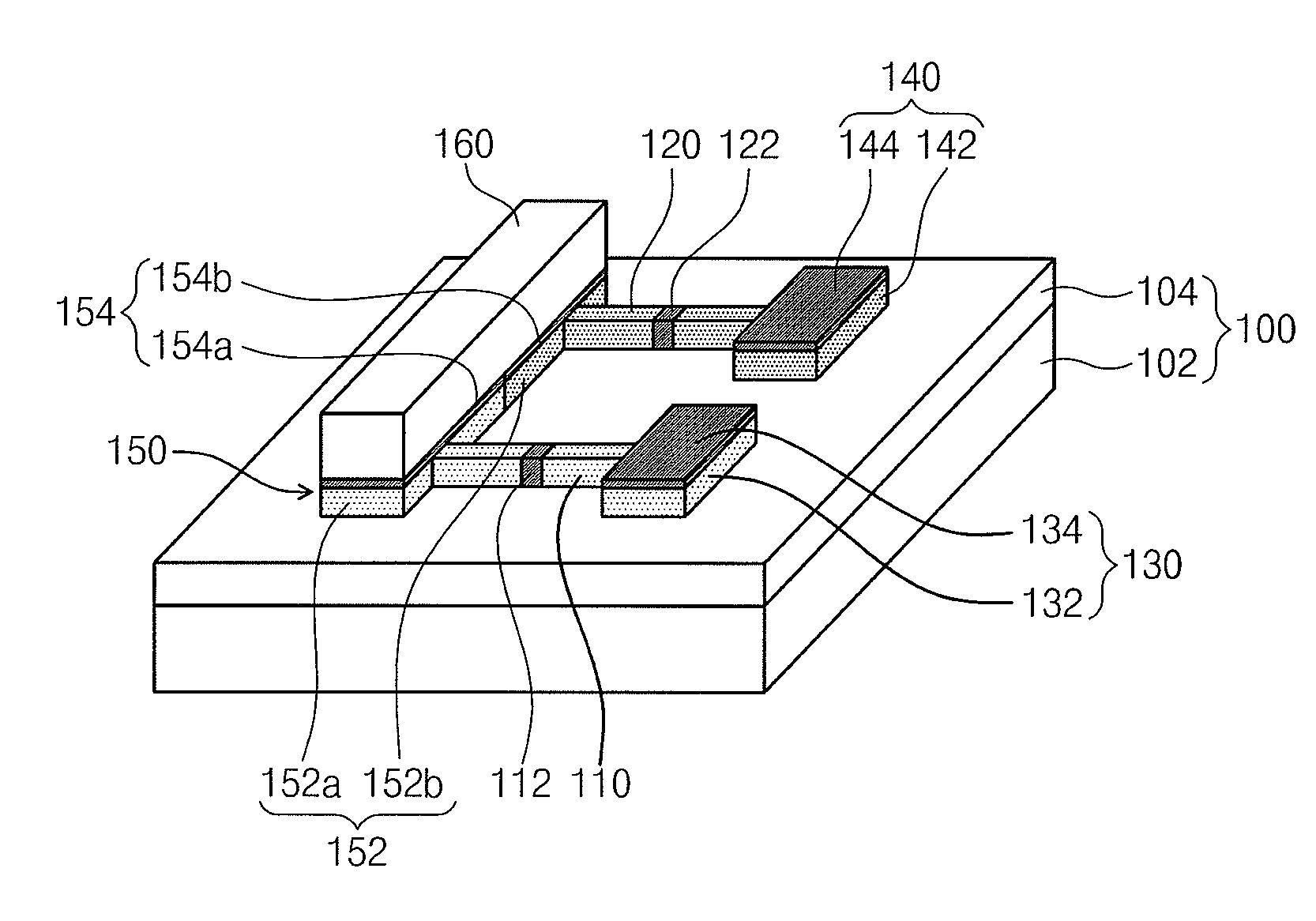
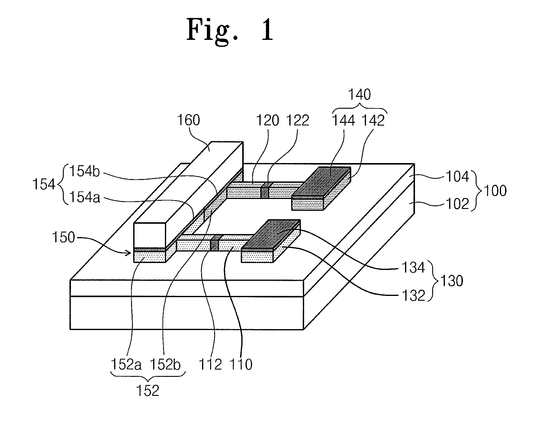
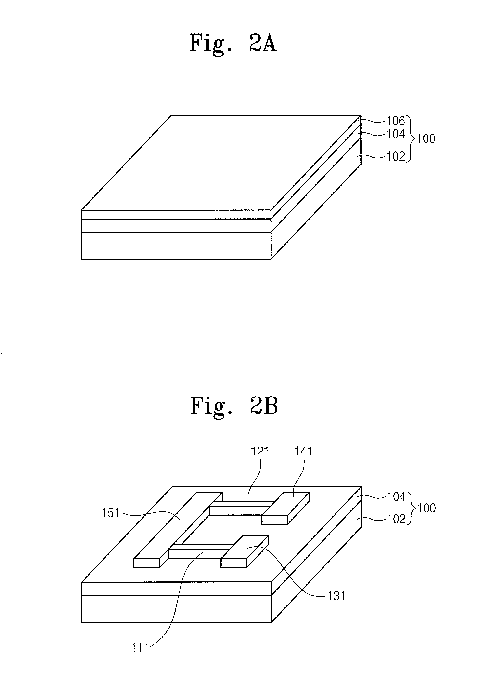
Provided are a thermoelectric device, a thermoelectric device module, and a method of forming the thermoelectric device. The thermoelectric device includes a first conductive type first semiconductor nanowire including at least one first barrier region; a second conductive type second semiconductor nanowire including at least one second barrier region; a first electrode connected to one end of the first semiconductor nanowire; a second electrode connected to one end of the second semiconductor nanowire; and a common electrode connected to the other end of the first semiconductor nanowire and the other end of the second semiconductor nanowire. The first barrier region is greater than the first semiconductor nanowire in thermal conductivity, and the second barrier region is greater than the second semiconductor nanowire in thermal conductivity.

Description

CROSS-REFERENCE TO RELATED APPLICATIONS[0001]This U.S. non-provisional patent application claims priority under 35 U.S.C. §119 of Korean Patent Application No. 10-2008-0118110, filed on Nov. 26, 2008, the entire contents of which are hereby incorporated by reference.BACKGROUND OF THE INVENTION[0002]The present invention disclosed herein relates to a thermoelectric device, and more particularly, to a thermoelectric device including semiconductor nanowires.[0003]The thermoelectric effect, discovered by Thomas Seebeck in 1821, has been widely applied to industries from the 1950s, together with discovering new semiconductor materials. Typically, materials generating the thermoelectric effect include Bi2Te3 that has a figure-of-merit (ZT) close to 1. However, heavy metals are used for the thermoelectric devices including Bi2Te3, and the thermoelectric devices including Bi2Te3 are very difficult to recycle. In addition, the thermoelectric devices including Bi2Te3 may cause environmental p...

Claims


Application Information

Patent Timeline
IPC IPC(8): H01L35/02H01L21/02
CPCH01L35/34H01L35/32H10N10/01H10N10/17B82Y40/00H10N10/80H10N10/00
Inventor JANG, MOON-GYUJUN, MYUNG-SIMROH, TAE-MOONKIM, JONG-DAEZYUNG, TAE-HYOUNG
Owner ELECTRONICS & TELECOMM RES INST
Learn More