Chip package structure

a technology of chip package and chip shell, which is applied in the direction of semiconductor devices, semiconductor/solid-state device details, electrical devices, etc., can solve the problems of complex fabrication process of the conventional chip package structure b>100/b>, and achieve the effect of increasing the clearance distance between leads and heat dissipation devices and the creepage distan

Active Publication Date: 2010-05-13
CYNTEC
View PDF2 Cites 15 Cited by
  • Summary
  • Abstract
  • Description
  • Claims
  • Application Information

AI Technical Summary

Benefits of technology

[0010]Accordingly, the present invention is directed to a chip package structure, wherein the creepage distance and the clearance distance between leads and a heat dissipa

Problems solved by technology

However, the fabrication process of the conventional chip package structure 100 is very complicated, and since the casing 140 and the chip

Method used


Image

  • Chip package structure
  • Chip package structure
  • Chip package structure

Examples


Embodiment Construction

[0030]Reference will now be made in detail to the present preferred embodiments of the invention, examples of which are illustrated in the accompanying drawings. Wherever possible, the same reference numbers are used in the drawings and the description to refer to the same or like parts.

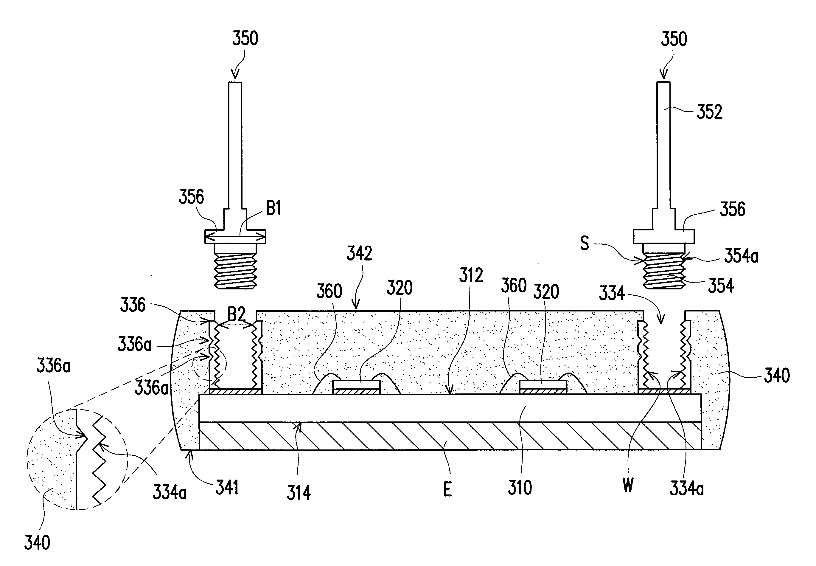
[0031]FIG. 3A is a cross-sectional view of a chip package structure according to an embodiment of the present invention, and FIG. 3B is an exploded view of the chip package structure in FIG. 3A. Referring to both FIG. 3A and FIG. 3B, in the present embodiment, the chip package structure 300 includes a substrate 310, a plurality of chips 320, a heat dissipation device E, a plurality of first conductive bars 330, a molding compound 340, and a plurality of second conductive bars 350.

[0032]The substrate 310 has two surfaces 312 and 314 which are opposite to each other. The substrate 310 may be a direct copper bonding substrate, a printed circuit substrate, a direct aluminium bonding substrate, an insulat...


PUM


Abstract

A chip package structure including a substrate, at least one chip, a heat dissipation device, at least one first conductive bar, a molding compound, and at least one second conductive bar is provided. The chip and the heat dissipation device are respectively disposed on a first and a second surface of the substrate. The first conductive bar has two opposite end surfaces, wherein one end surface is disposed on the first surface of the substrate, the other end surface is extended away from the substrate, and a fastening slot is disposed between the two end surfaces and passes through the other end surface. The molding compound encapsulates the substrate, the chip, part of the heat dissipation device, and the first conductive bar. The second conductive bar is disposed on one surface of the molding compound and has a protrusion portion fastened to the fastening slot of the first conductive bar.

Description

CROSS-REFERENCE TO RELATED APPLICATION[0001]This application claims the priority benefit of Taiwan application serial no. 97143525, filed on Nov. 11, 2008. The entirety of the above-mentioned patent application is hereby incorporated by reference herein and made a part of specification.BACKGROUND OF THE INVENTION[0002]1. Field of the Invention[0003]The present invention generally relates to a chip package structure, and more particularly, to a chip package structure with high voltage protection.[0004]2. Description of Related Art[0005]When a chip package structure with high-voltage input (for example, a power module for controlling a power supply or an IGBT module for controlling a driving motor) is designed, in order to make sure that the chip package structure meets the safety specification (for example, the UL standard) and works properly, the creepage distance and clearance distance between a voltage input terminal (for example, a lead) and a metal material (for example, a heat ...

Claims


Application Information

Patent Timeline
IPC IPC(8): H01L23/48
CPCH01L23/36H01L24/48H01L23/49811H01L24/45H01L24/49H01L2224/32225H01L2224/45144H01L2224/48091H01L2224/48227H01L2224/48247H01L2224/49H01L2224/73265H01L2924/01013H01L2924/01014H01L2924/01029H01L2924/01074H01L2924/01079H01L2924/01082H01L2924/13055H01L2924/15312H01L2924/1532H01L23/3735H01L2224/48137H01L2924/01023H01L2924/1305H01L2924/01033H01L2924/00014H01L2924/00H01L2924/00012H01L2924/1815H01L2924/181H01L24/73
Inventor LU, BAU-RUWEN, CHAU-CHUNCHEN, DA-JUNGLU, CHUN-HSIEN
Owner CYNTEC
Why Eureka
Try Eureka