Organic el device and electronic apparatus
- Summary
- Abstract
- Description
- Claims
- Application Information
AI Technical Summary
Benefits of technology
Problems solved by technology
Method used
Image
Examples
experimental examples
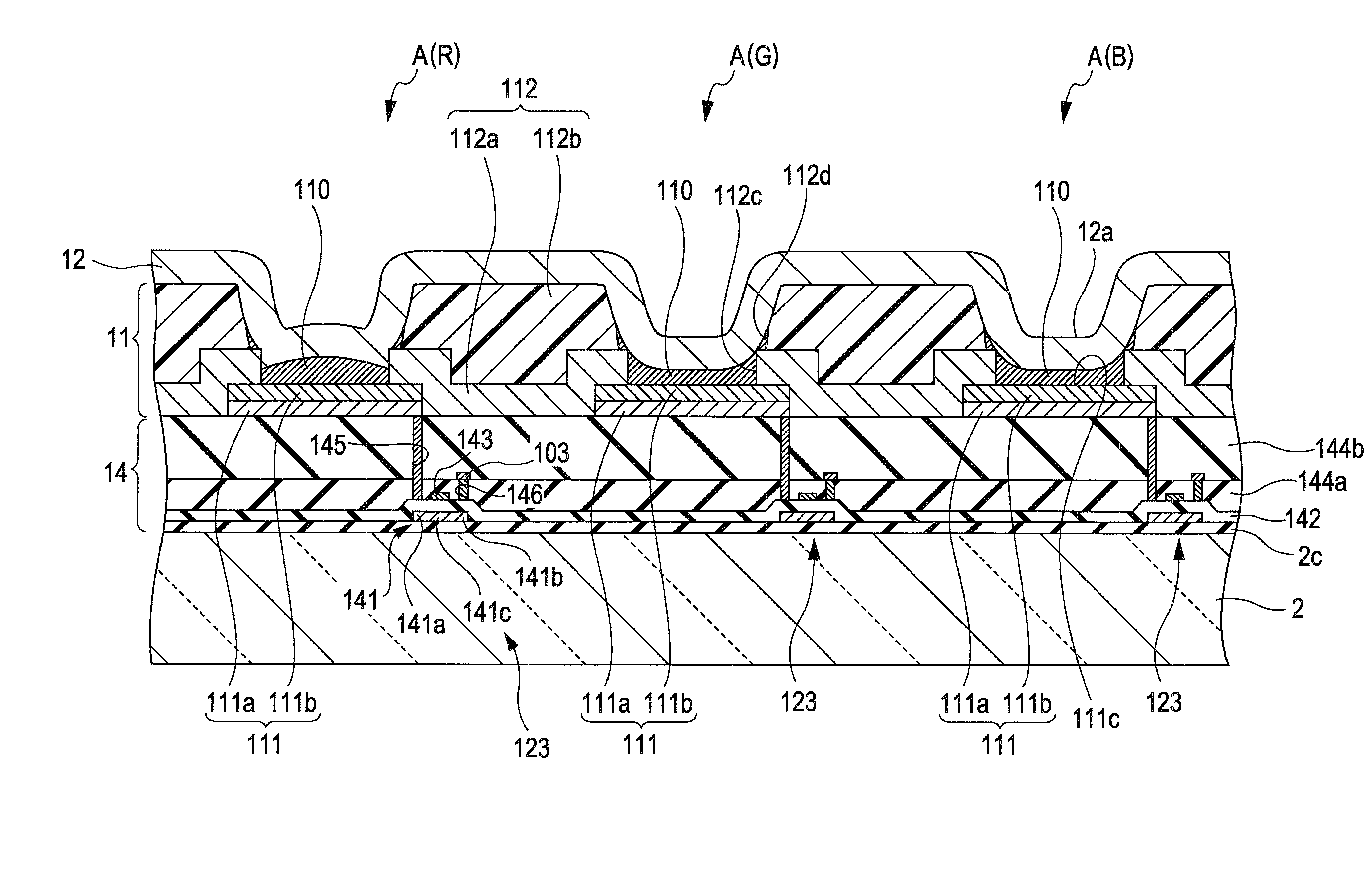
[0112]The relationship between the film thickness of the light emitting layer and the current efficiency of the light emitting element (organic EL element) was checked in the following manner.
[0113]As the light emitting element (organic EL element), the anode was formed to have the same configuration as shown in FIGS. 3 and 4 without forming a partition wall on a glass substrate, and a hole injection layer and a hole transport layer were formed by using a spin-coat method. In addition, the above-described red light emitting material was coated thereon by using the spin-coat method, and a light emitting layer was formed so as to acquire a functional layer. Thereafter, a cathode was formed on the light emitting layer so as to form a light emitting element (organic EL element).
[0114]Then, the thickness of the light emitting element (organic EL element), in particular, the thickness of the light emitting layer was changed with maintaining the other configurations, whereby light emitting...
PUM
 Abstract
Description
Claims
Application Information
 - R&D
- Intellectual Property
- Life Sciences
- Materials
- Tech Scout
- Unparalleled Data Quality
- Higher Quality Content
- 60% Fewer Hallucinations
Browse by: Latest US Patents, China's latest patents, Technical Efficacy Thesaurus, Application Domain, Technology Topic, Popular Technical Reports.
© 2025 PatSnap. All rights reserved.Legal|Privacy policy|Modern Slavery Act Transparency Statement|Sitemap|About US| Contact US: help@patsnap.com


