Semiconductor memory device and data write method thereof

Active Publication Date: 2010-03-11
KIOXIA CORP
View PDF6 Cites 32 Cited by
  • Summary
  • Abstract
  • Description
  • Claims
  • Application Information

AI Technical Summary

Benefits of technology

[0008]According to an aspect of the present invention, there is provided a semiconductor memory device comprising: a memory cell array including a plurality of memory cells which are arranged in a matrix at intersections between a plurality of word lines and a plurality of bit lines; a word line driving circuit which applies a voltage to the word lines; a bit line control circuit including a buffer which retains a verify result of the memory cell array, and a bit scan c

Problems solved by technology

However, the decrease in write step voltage (dVPGM) leads to an increase in the number of times of data write, that is, an increase in program time (tPROG).
In this trend, one problem is how to shorten a write time, while ensuring reliability.

Method used


Image

  • Semiconductor memory device and data write method thereof
  • Semiconductor memory device and data write method thereof
  • Semiconductor memory device and data write method thereof

Examples


first embodiment

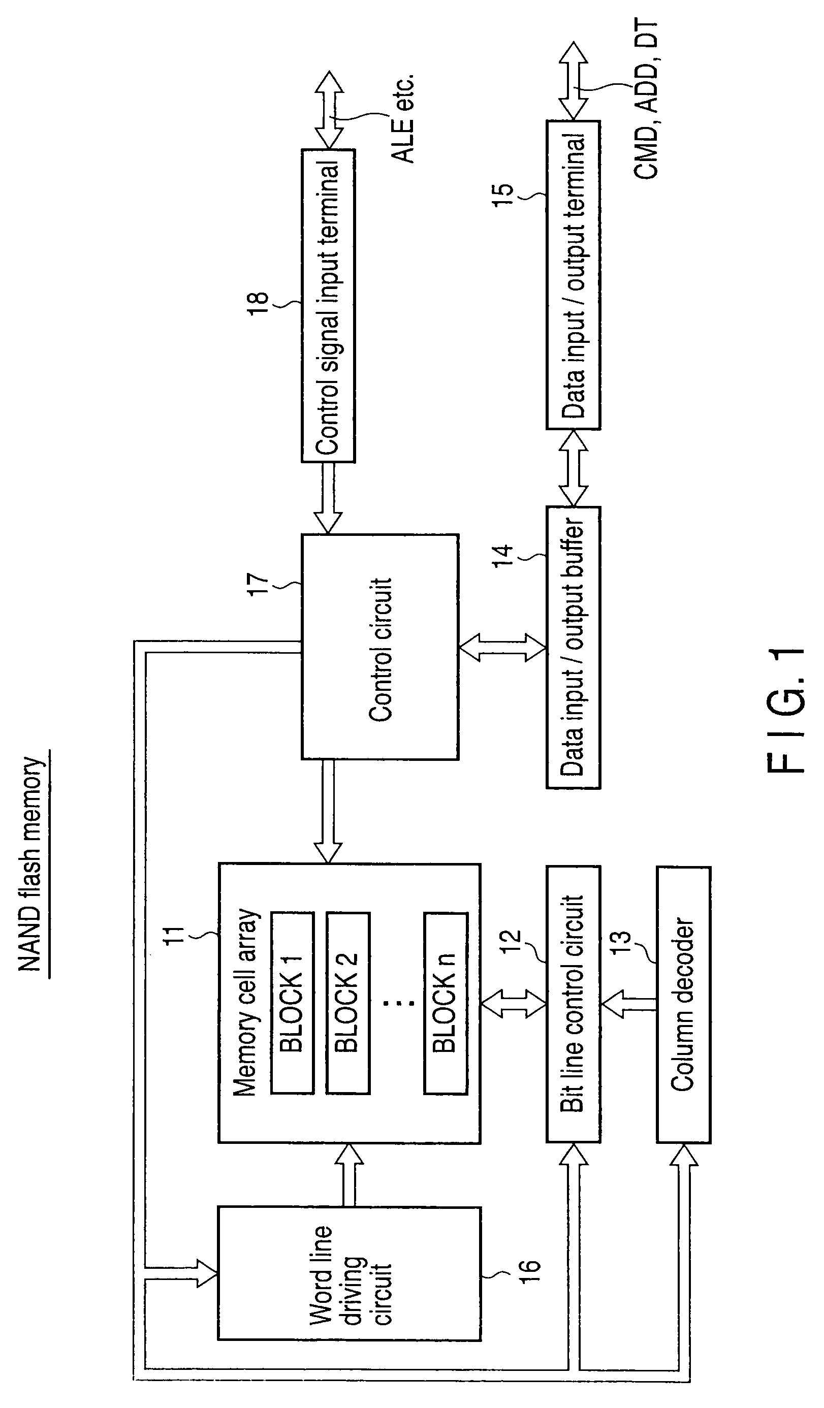
[0044]To begin with, referring to FIG. 1 to FIG. 6, a description is given of a structure example of the NAND flash memory according to the first embodiment of the present invention.

1-1. Example of Entire Structure

[0045]FIG. 1 shows an example of the entire structure of the NAND flash memory according to the first embodiment.

[0046]As shown in FIG. 1, the NAND flash memory according to this embodiment comprises a memory cell array 11, a bit line control circuit 12, a column decoder 13, a data input / output buffer 14, a data input / output terminal 15, a word line driving circuit 16, a control circuit 17, and a control signal input terminal 18.

[0047]The memory cell array 11 is composed of a plurality of blocks (BLOCK1 to BLOCKn). The word line driving circuit 16 for controlling word lines and the bit line control circuit 12 for controlling bit lines are connected to the memory cell array 11.

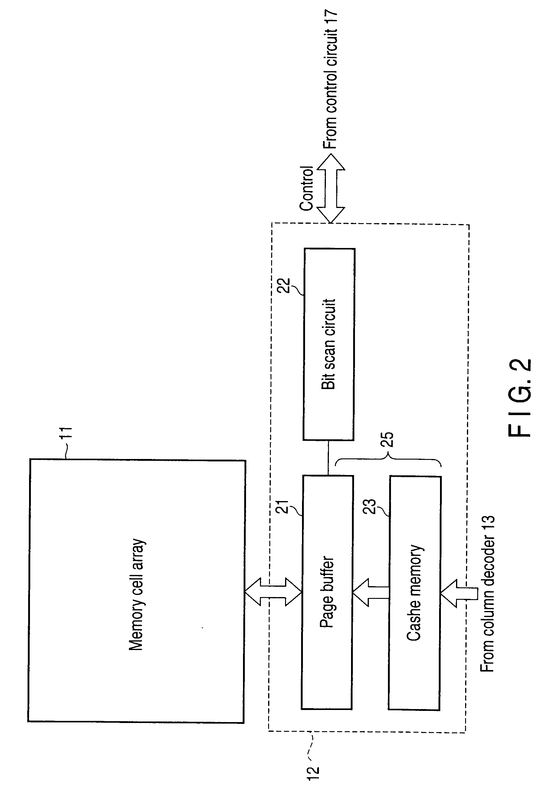
[0048]The bit line control circuit 12 reads data of memory cell transistors in the memory cell arr...

second embodiment (

[Second Embodiment (An Example in Which Data Write is Executed from a Central Threshold Voltage Level Side)]

[0209]Next, referring to FIG. 22 to FIG. 25, a description is given of a semiconductor memory device according to a second embodiment of the invention and a data write method thereof. This embodiment relates to an example in which the control circuit 17 executes control to perform data write from a threshold voltage level (the central 8th value Lev08 in this example) side, which is higher than the lowest threshold voltage level (Lev00) of the multilevel data (16 values Lev00 to Lev15 in this example). In this description, a detailed description of the parts common to those in the first embodiment is omitted.

[0210]Referring to FIG. 22 to FIG. 26, a description is given of the data write operation of the semiconductor memory device according to the second embodiment.

[0211]The second embodiment differs from the first embodiment in that in the above-described step S2-2, the data w...


PUM


Abstract

A semiconductor memory device includes a control circuit. The control circuit executes control to perform a verify operation with respect to only a lowest threshold voltage level of a memory cell at a time of a data write operation, and to skip the verify operation with respect to the other threshold voltage levels. The control circuit determines whether a verify pass bit number of the lowest threshold voltage level, which is counted by a bit scan circuit, is a prescribed bit number or more, and the control circuit further executes control, if the verify pass bit number is the prescribed bit number or more, to perform the verify operation with respect to only the lowest threshold voltage level and a threshold voltage level that is higher than the lowest threshold voltage level, and to skip the verify operation with respect to the other threshold voltage levels.

Description

CROSS-REFERENCE TO RELATED APPLICATIONS[0001]This application is based upon and claims the benefit of priority from prior Japanese Patent Application No. 2008-230295, filed Sep. 8, 2008, the entire contents of which are incorporated herein by reference.BACKGROUND OF THE INVENTION[0002]1. Field of the Invention[0003]The present invention relates to a semiconductor memory device and a data write method thereof, and is applied, for example, to a NAND flash memory.[0004]2. Description of the Related Art[0005]In a data write operation of a NAND flash memory, for example, a program loop is repeated with an arbitrary step width, and the program loop is stopped when data write in all bits is finished.[0006]With the development of multilevel implementation of NAND flash memories, it becomes necessary to more finely control the intervals of data write levels of memory cells. It is thus necessary to make a write step voltage (dVPGM) lower. However, the decrease in write step voltage (dVPGM) le...

Claims


Application Information

Patent Timeline
IPC IPC(8): G11C16/04G11C16/06
CPCG11C11/5628G11C16/0483G11C16/24G11C16/3459G11C16/10G11C2211/5621G11C16/08G11C16/30G11C16/34
Inventor KOMATSU, YUKIO
Owner KIOXIA CORP
Why Eureka
Try Eureka