Data writing method for flash memory and storage system and controller using the same

Active Publication Date: 2009-12-10
PHISON ELECTRONICS
View PDF8 Cites 40 Cited by
  • Summary
  • Abstract
  • Description
  • Claims
  • Application Information

AI Technical Summary

Benefits of technology

[0008]Accordingly, the present invention is directed to a data writing method which ensures the accuracy of data written by a previous writing command when a programming error occurs to a multi-level cell (MLC) NAND flash memory.
[0034]According to the data writing method in the present invention, a data is only written into lower page addresses or upper page addresses corresponding to the lower page addresses which do not store any valid data written by a previous writing command in a MLC NAND flash memory. Thereby, the data written by the previous writing command is not affected even when a programming error occurs to the current writing command, and accordingly the system is prevented from using incorrect data.

Problems solved by technology

Due to the physical characteristics of MLC NAND flash memory, the voltage is not very stable when some page addresses thereof are programmed and which may further affect the adjoining page addresses.
Accordingly, even though a MLC NAND flash memory can provide larger storage capacity, the storage reliability thereof is not very satisfactory.
In other words, the data written by a previous writing command may be damaged when a programming error occurs to a page address written by a current writing command.

Method used


Image

  • Data writing method for flash memory and storage system and controller using the same
  • Data writing method for flash memory and storage system and controller using the same
  • Data writing method for flash memory and storage system and controller using the same

Examples


Embodiment Construction

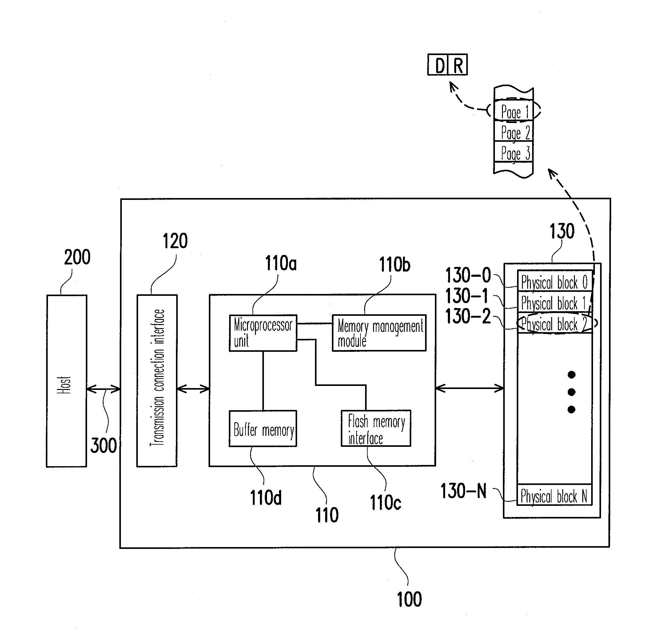
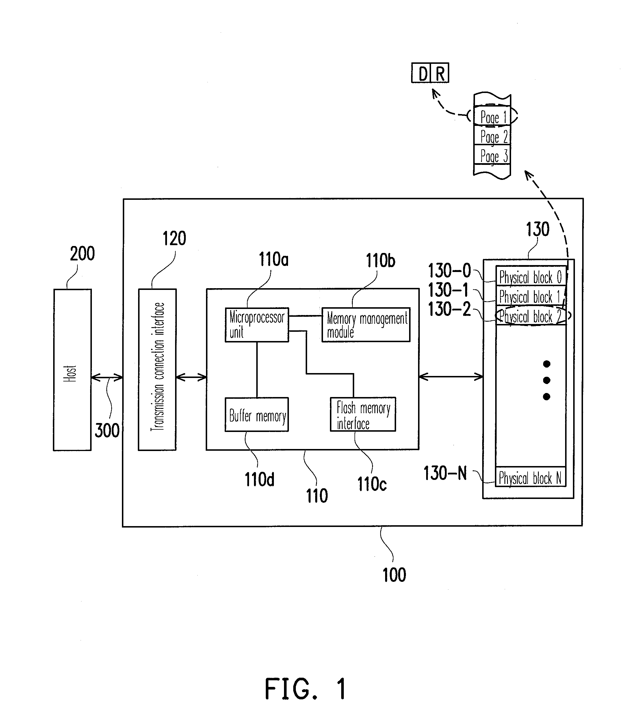
[0043]Reference will now be made in detail to the present preferred embodiments of the invention, examples of which are illustrated in the accompanying drawings. Wherever possible, the same reference numbers are used in the drawings and the description to refer to the same or like parts.

[0044]FIG. 1 is a schematic block diagram of a flash memory storage system according to an embodiment of the present invention. Referring to FIG. 1, the flash memory storage system 100 includes a controller 110, a transmission connection interface 120, and a flash memory 130.

[0045]The flash memory storage system 100 is usually used together with a host 200 so that the host 200 can write data into the flash memory storage system 100 or read data from the flash memory storage system 100. In the present embodiment, the flash memory storage system 100 is a solid state drive (SSD). However, in another embodiment of the present invention, the flash memory storage system 100 may also be a flash memory card ...


PUM


Abstract

A data writing method for a multi-level cell (MLC) NAND flash memory and a storage system and a controller using the same are provided. The flash memory includes a plurality of blocks. Each of the blocks includes a plurality of page addresses. The page addresses are categorized into a plurality of upper page addresses and a plurality of lower page addresses. The writing speed of the lower page addresses is faster than that of the upper page addresses. The data writing method includes receiving a writing command and data and writing the data into a page address. The page address is skipped when it is an upper page address and a corresponding lower page address stores a valid data written by a previous writing command. Thereby, the accuracy of the data written by the previous writing command is ensured when a programming error occurs to the flash memory.

Description

CROSS-REFERENCE TO RELATED APPLICATION[0001]This application claims the priority benefit of Taiwan application serial no. 97121383, filed on Jun. 9, 2008. The entirety of the above-mentioned patent application is hereby incorporated by reference herein and made a part of this specification.BACKGROUND[0002]1. Technology Field[0003]The present invention generally relates to a data writing method, and more particularly, to a data writing method for writing data into a multi-level cell (MLC) NAND flash memory and a storage system and a controller using the same.[0004]2. Description of Related Art[0005]Along with the widespread of digital cameras, camera phones, and MP3 in recently years, the consumers' demand to storage media has increased drastically too. Flash memory is one of the most adaptable memories for such battery-powered portable products due to its characteristics such as data non-volatility, low power consumption, small volume, and non-mechanical structure. Besides being app...

Claims


Application Information

Patent Timeline
IPC IPC(8): G06F12/02
CPCG06F12/0246G06F2212/1032G06F2212/7202G11C16/105G11C16/0483G11C16/10G11C11/5628
Inventor CHU, CHIEN-HUA
Owner PHISON ELECTRONICS
Why Eureka
Try Eureka