
Contactless Programming and Testing of Memory Elements

a technology of memory elements and programming, applied in the field of contactless programming and testing of memory elements, can solve problems such as memory or file system corruption, and achieve the effects of saving costs, improving flexibility, and improving the production of devices

Active Publication Date: 2009-12-03
III HLDG 3
View PDF14 Cites 115 Cited by
  • Summary
  • Abstract
  • Description
  • Claims
  • Application Information

AI Technical Summary

Benefits of technology

[0012]The method according to the invention enables the replacement of direct physical connections for the programming of memory modules, e.g. during manufacturing of an electronic device or component. This provides improved flexibility, as the programming can be performed at any time and at any location within the manufacturing and logistics chain. The reduction or even omission of physical contacts can also improve immunity of the memory modules against electrostatic discharges. The wireless interface replacing the conventional direct connections can also be used later on for debugging / testing purposes, and even in the logistics channels for altering system software or likes without opening the package.
[0048]According to an exemplary embodiment the manufacturing comprises an assembly step of hardware components including said memory element, and wherein said method for programming said memory element is performed before, during or after said assembly step. The flexibility of performing the programming independent from the actual stage of the device assembly process can improve the production of devices with respect to required production time and also help save costs.

Problems solved by technology

This malfunction is usually caused by some damaged component other than memory, e.g. if physical interface such as a pad connection is damaged by corrosion caused by humidity, and / or the program memory or file system is corrupted.

Method used


Image

  • Contactless Programming and Testing of Memory Elements
  • Contactless Programming and Testing of Memory Elements
  • Contactless Programming and Testing of Memory Elements

Examples


Embodiment Construction

[0084]An RFID system generally comprises an interrogator (or sometimes called a reader) and one or more tags (or sometime called transponders). In addition to the reading capability the RFID interrogator may also act as a writer. In the ideal case the power which is needed to operate and read / write data to / from these tags is transferred from the interrogator to the tag via electromagnetic fields; therefore the tag can operate without its own power supply (e.g. battery). This kind of a system is called a passive RFID system and it usually requires a fairly constant power transfer from the interrogator. Another option is the use of semi-passive tags wherein power is supplied from its own power source, but the electromagnetic field generated by the interrogator is used for transferring data from the tag to the interrogator. Thus more energy can be reflected back (backscattering) to the interrogator, due to the fact that the energy is not needed for the tag. A third category comprises a...


PUM


Abstract

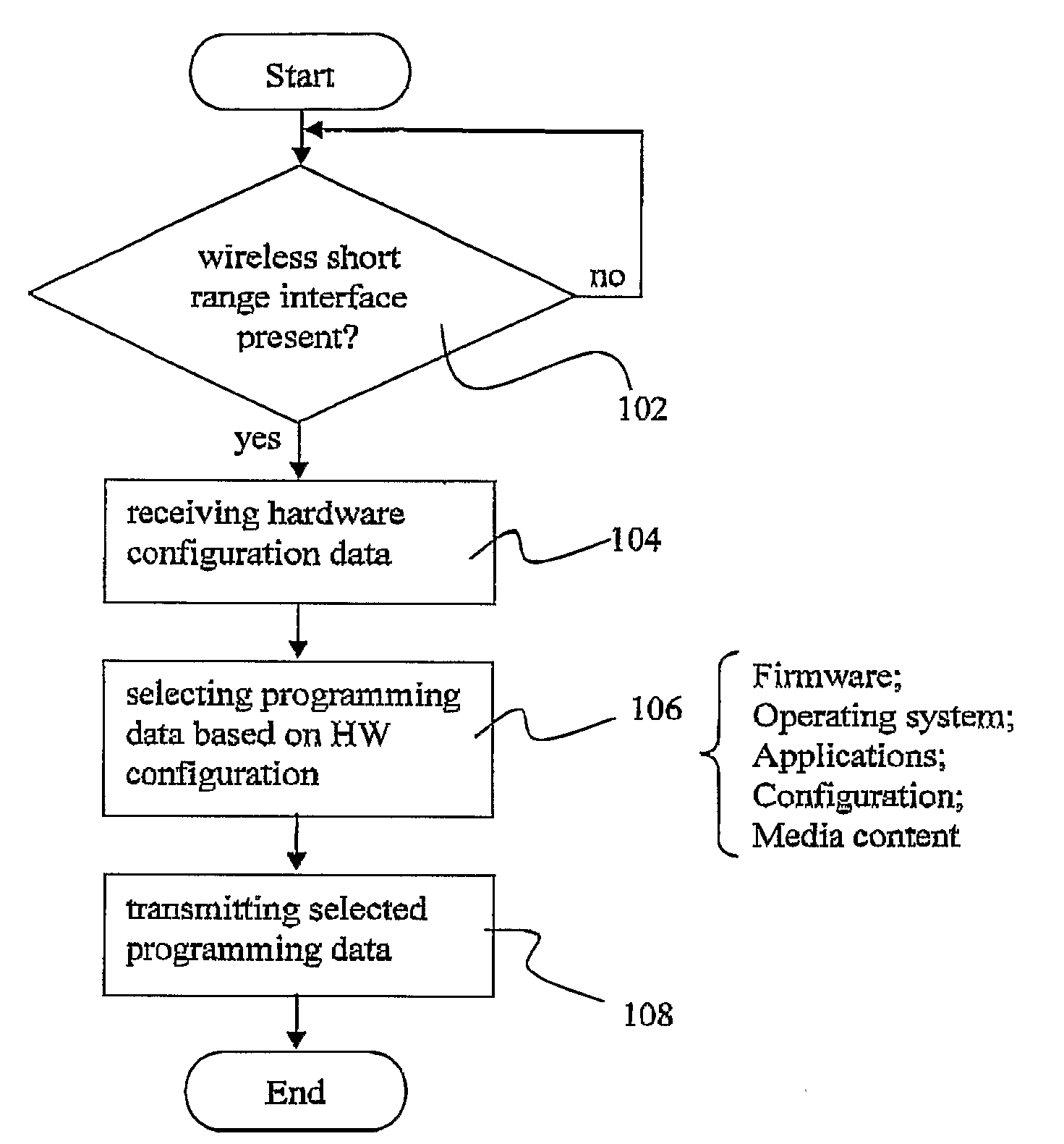
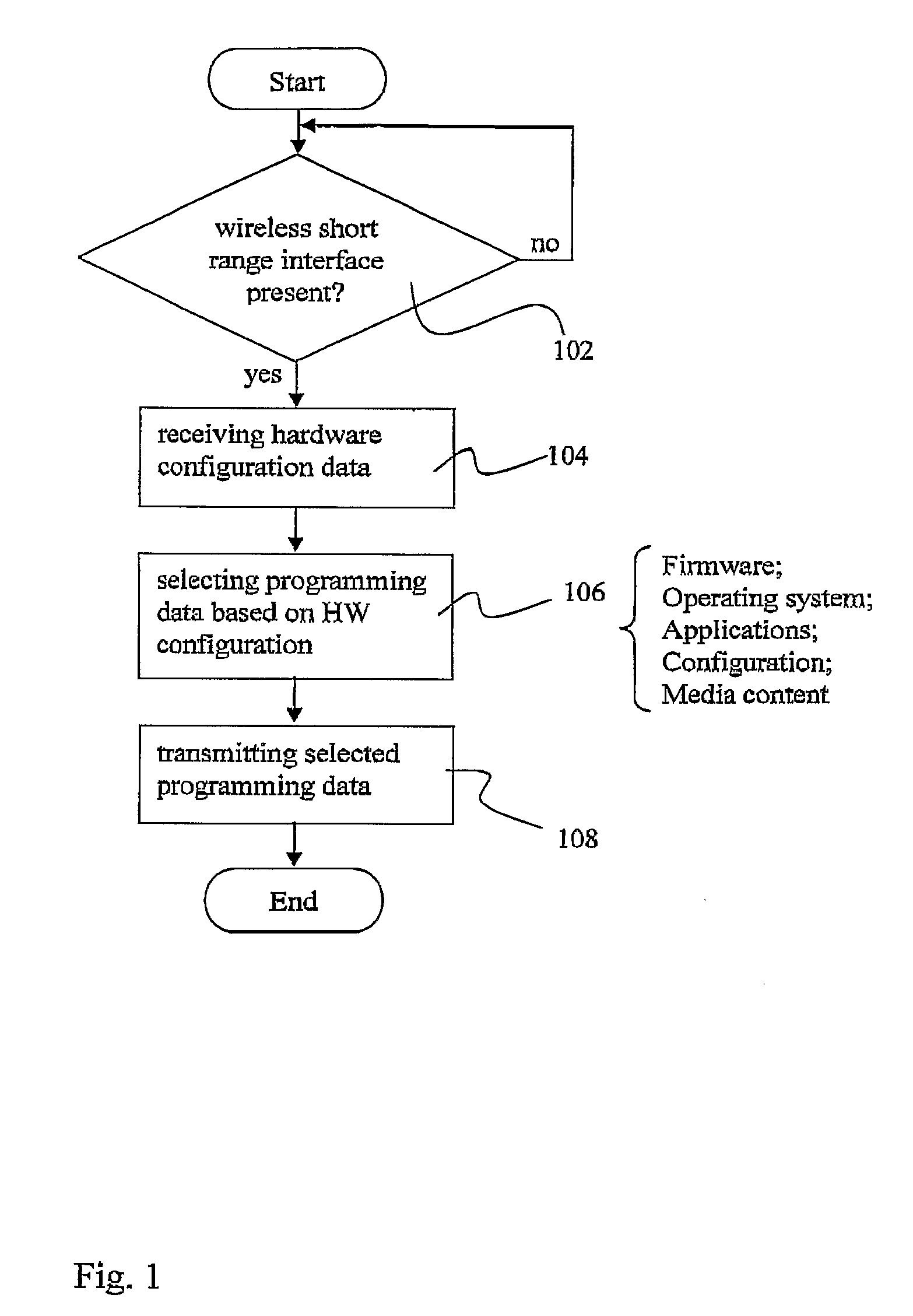
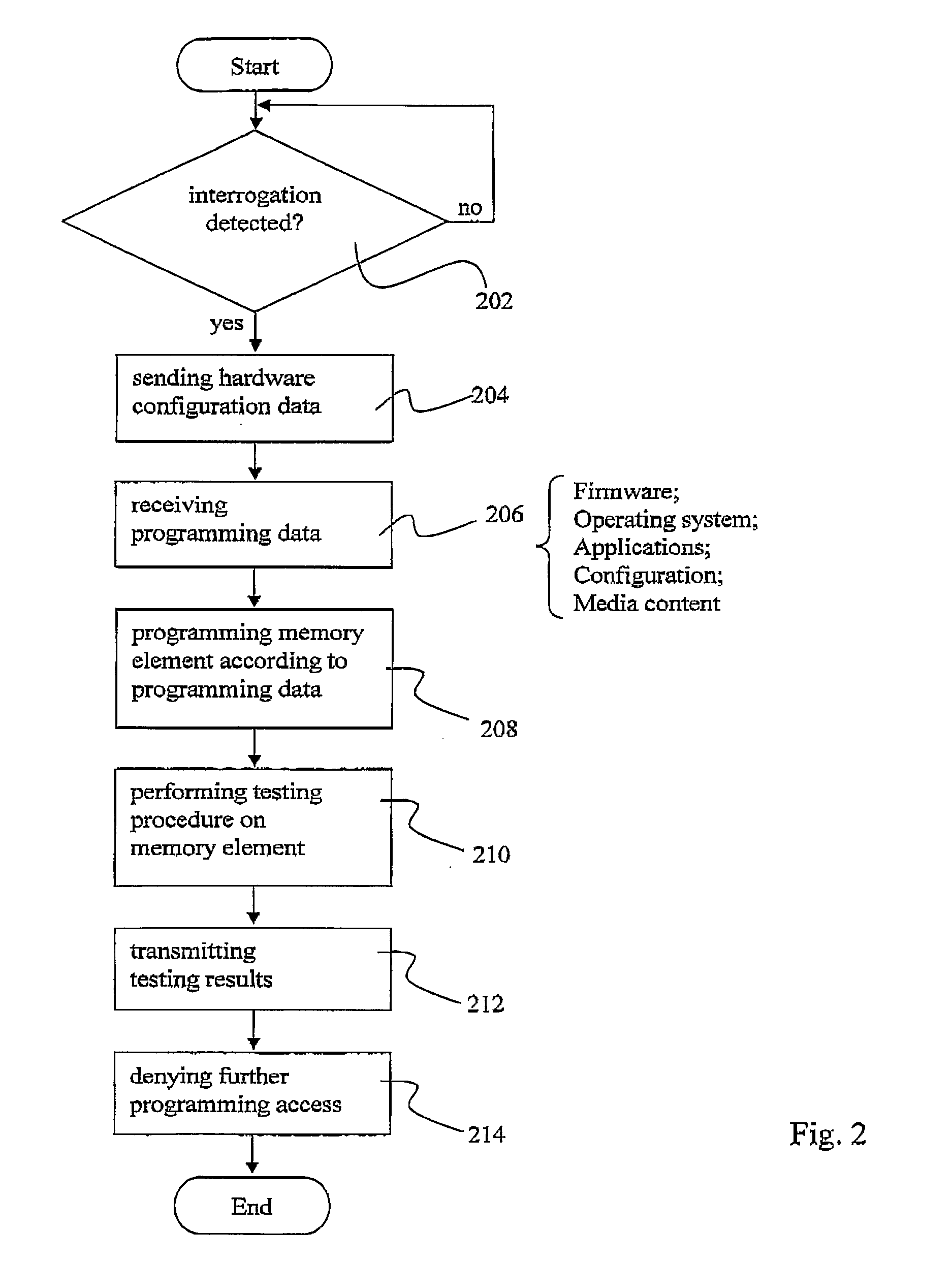
The present invention provides a method for contactless programming of a memory element of an electronic device having a wireless short range communications interface. The method comprises performing an interrogation for detecting the presence of said wireless short range communications interface, receiving, responsive to said interrogation, data from said wireless interface, said data indicating a hardware configuration of said electronic device, selecting programming data for programming said memory element based on said hardware configuration, and transmitting said selected programming data to be received by said wireless short range communications interface. The method further comprises detecting an interrogation, transmitting, responsive to said interrogation, data via said wireless interface, said data indicating a hardware configuration of said electronic device, receiving programming data at said wireless short range communications interface, and programming said memory element according to said programming data. The invention also provides devices for performing the inventive method.

Description

[0001]This invention is related to methods and devices for performing programming, configuring, debugging and / or testing of memory components in a contactless manner.PRIOR ART[0002]The manufacturing of a number of modern devices including electronic equipment, e.g. mobile terminals etc., requires permanent and / or temporary programming of memory components with certain information. This includes information like firmware, operating system, application software, market specific configuration data, logistics data and media content.[0003]Current solutions for downloading software onto a device during manufacturing, e.g. flashing a flash ROM, are performed by using a mechanism that requires preliminary flashing algorithms to be present on the device, a physical connection and a connected power supply. The software download into products is conventionally performed in a programming station at the end of the manufacturing line after all components have been placed in the products. The soft...

Claims


Application Information

Patent Timeline
IPC IPC(8): H04Q5/22H04L67/125H04M1/72406H04M1/72412
CPCG06F8/61G06F8/64H04M1/24H04L67/125H04M1/7253H04W8/245H04L67/34H04M1/72525G06F8/654H04M1/72406H04M1/72412H04L12/28H04B7/24
Inventor RONKKA, RISTOREUNAMAKI, JUKKA
Owner III HLDG 3
Learn More