
Deuterated Semiconducting Organic Compounds for Use in Light-Emitting Devices

a semiconducting organic compound and light-emitting device technology, applied in the direction of organic chemistry, group 3/13 element organic compounds, discharge tube luminescnet screens, etc., can solve the problems of low light emission efficiency, poor high-voltage stability, and organic light-emitting materials, so as to prolong the use life of the light-emitting device, reduce the turn-on voltage, and increase the voltage stability

Inactive Publication Date: 2009-12-03
HWANG KUO CHU
View PDF3 Cites 29 Cited by
  • Summary
  • Abstract
  • Description
  • Claims
  • Application Information

AI Technical Summary

Benefits of technology

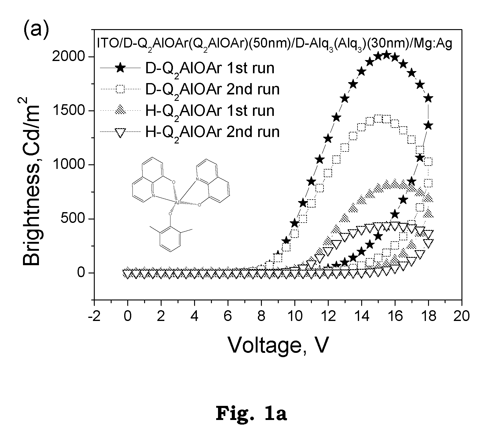
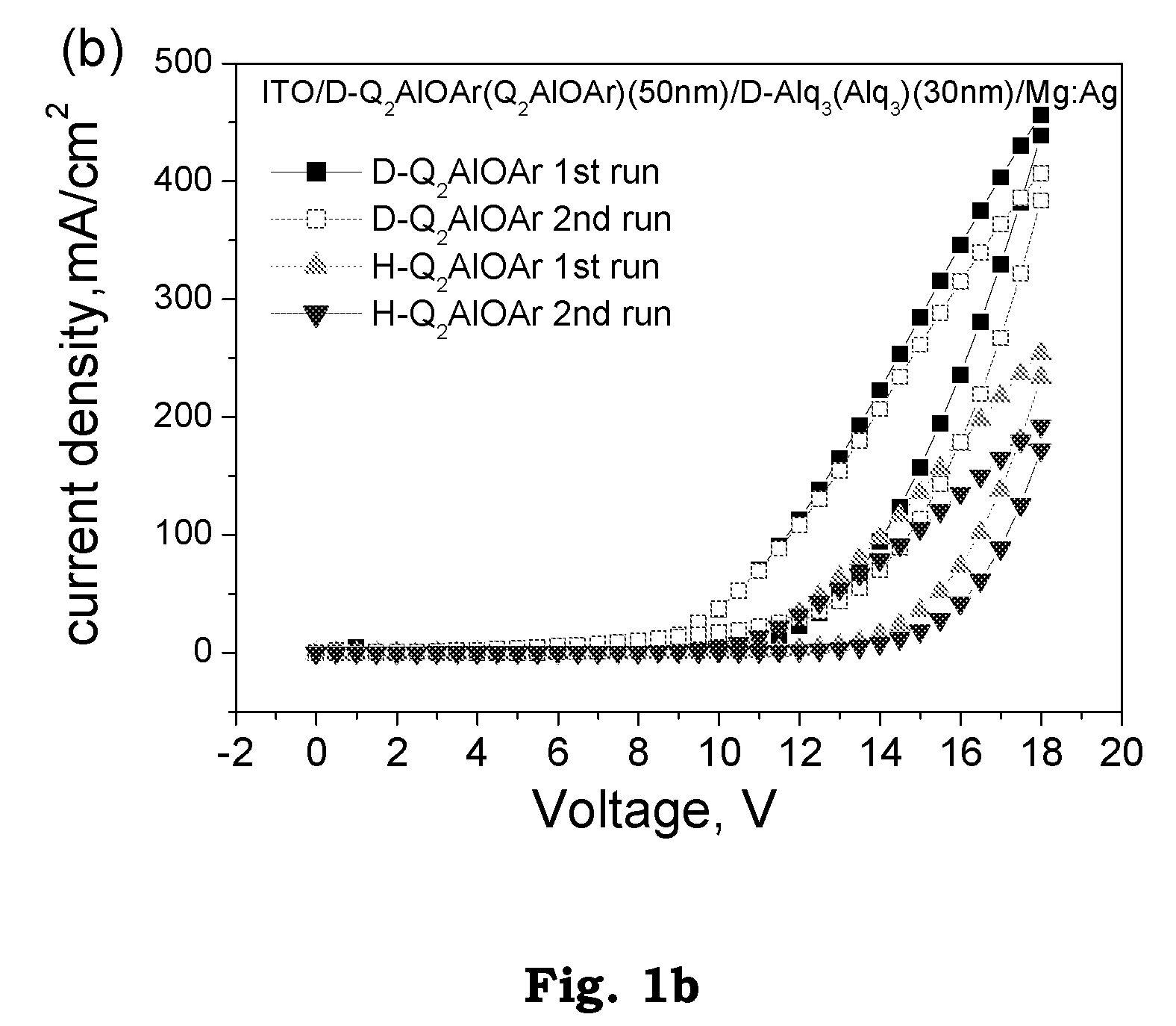
[0006]One object of the present invention is to employ deuterated semiconducting organic compounds for using in light-emitting devices. By partially or fully deuterated the protons of the semiconducting organic compounds, the high voltage stability of the light-emitting devices can be increased, and the turn-on voltage can be decreased. Thus, the usage lifetime of the light-emitting devices can be prolonged efficiently.
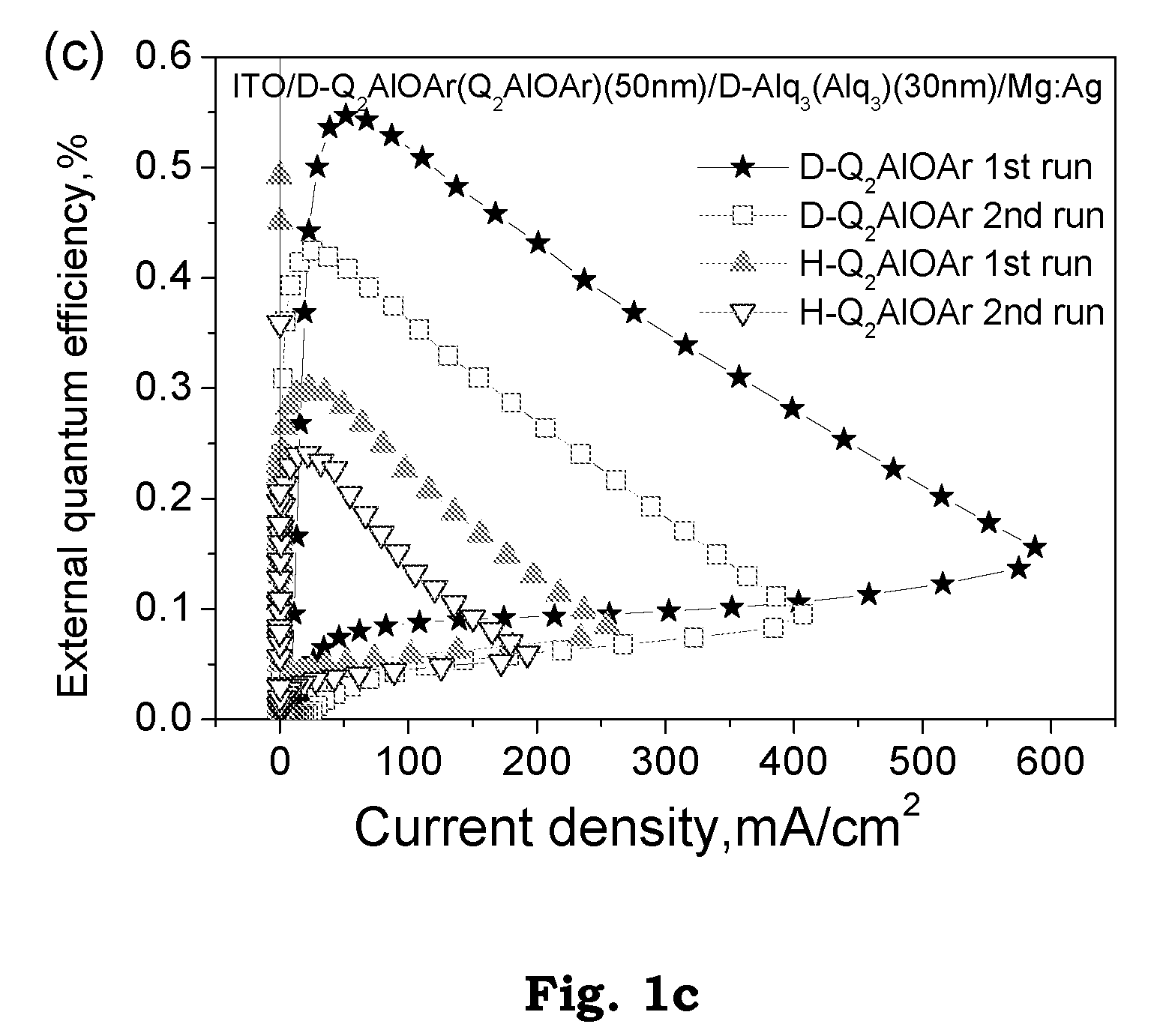
[0007]Another object of the present invention is to employ deuterated semiconducting organic compounds for using in light-emitting devices. By partially or fully deuterated the protons of the semiconducting organic compounds, the external quantum efficiency and the light emission efficiency of the light-emitting materials can be increased, and thus, the luminance efficiency of the light-emitting devices can be improved.

Problems solved by technology

Although having many advantages, organic light-emitting materials still suffer from some drawbacks, such as low light emission efficiency and poor high-voltage stability.

Method used


Image

  • Deuterated Semiconducting Organic Compounds for Use in Light-Emitting Devices
  • Deuterated Semiconducting Organic Compounds for Use in Light-Emitting Devices
  • Deuterated Semiconducting Organic Compounds for Use in Light-Emitting Devices

Examples


Embodiment Construction

[0010]What is probed into the invention is organometallic complexes and their application. Detail descriptions of the structure and elements will be provided in the following in order to make the invention thoroughly understood. Obviously, the application of the invention is not confined to specific details familiar to those who are skilled in the art. On the other hand, the common structures and elements that are known to everyone are not described in details to avoid unnecessary limits of the invention. Some preferred embodiments of the present invention will now be described in greater detail in the following. However, it should be recognized that the present invention can be practiced in a wide range of other embodiments besides those explicitly described, that is, this invention can also be applied extensively to other embodiments, and the scope of the present invention is expressly not limited except as specified in the accompanying claims.

[0011]One preferred embodiment of thi...


PUM

PropertyMeasurementUnit
temperatureaaaaaaaaaa
pressureaaaaaaaaaa
thicknessaaaaaaaaaa

Abstract

The present invention discloses deuterated semiconducting organic compounds. The deuterated semiconducting organic compounds comprise at least one partially or fully deuterated non-conjugated portion linked to the conjugated portion. The mentioned deuterated semiconducting organic compounds can be used in optoelectronic devices, such as light-emitting devices and photodiodes, with enhanced performance and lifetime. The deuterated semiconducting organic compounds of this application can be employed as emissive layer, charge-transporting layer, or energy transfer material in organic light-emitting devices.

Description

BACKGROUND OF THE INVENTION[0001]1. Field of the Invention[0002]The present invention is generally related to semiconducting organic compounds for use in optoelectronic devices, and more particularly to deuterated semiconducting organic compounds for use in light-emitting devices.[0003]2. Description of the Prior Art[0004]Organic light emitting diodes (OLEDs) are under intensive investigation because of their potential of achieving improved device performances. OLED has the advantages of self-light, wide view angles, being lightweight, fast response time, and low power consumption, etc. Although having many advantages, organic light-emitting materials still suffer from some drawbacks, such as low light emission efficiency and poor high-voltage stability. In view of the above matter, developing a novel organic compound having high voltage stability and low turn-on voltage to prolong the usage lifetime of the device and to increase luminance efficiency is still an important task for t...

Claims


Application Information

Patent Timeline
Patent Type & Authority Applications(United States)
IPC IPC(8): H01J1/63C07D403/10C07D491/16C07D471/06C07F1/00C07F3/00C07F5/00C07F7/00
CPCC07D209/86H05B33/14C07D491/16C07F5/069C09K11/06C09K2211/1011C09K2211/1029C09K2211/1033C09K2211/1037C09K2211/1088C09K2211/185C09K2211/186H01L51/0081H01L51/5012H01L51/5048C07D215/26H10K85/324H10K50/14H10K50/11
Inventor HWANG, KUO-CHUTONG, CHUN-CHIHYEH, TZU-HAO
Owner HWANG KUO CHU
Learn More